PAM-XIAMEN provides indium arsenide (InAs) ingot with high quality and competitive price. Indium arsenide is a group III-V compound semiconductor material composed of indium and arsenic. It is a silver-gray solid at room temperature, and the indium arsenide crystal structure is a zinc blende crystal structure with a lattice constant of 0.6058nm, and a density of 5.66g/cm (solid state), 5.90g/cm (liquid at the melting point). The indium arsenide energy band structure is a direct transition, and the band gap width (300K) is 0.45eV. At the melting point of InAs (942 degree), the dissociation pressure of arsenic is only 0.033MPa, and single crystals can be grown from the melt under normal pressure. Indium arsenide ingot has high electron mobility and mobility ratio (μe/μh=70), low magnetoresistance effect and small temperature coefficient of resistance. Thus, indium arsenide boule is an ideal material for manufacturing Hall devices and magnetoresistive devices. Below is the specification listed for your reference.

Lingot d'arséniure d'indium
1. Spécification du lingot d'arséniure d'indium (PAM210618-INAS)
| La méthode: | VGF |
| Orientation: | (111) |
| Diamètre: | 50,8 mm |
| Dopant: | non dopé |
| Type de conductivité : | De type N |
| CC (@77K): | <=3*10^16cm-3 |
| Mobilité: | >=18000 à température ambiante |
| EPD: | <5000 |
| Longueur de lingot : | >= 50mm |
Besides, indium arsenide polycrystalline ingot boule is available:
InAs Polycrystalline Crystal (PAM170324-INAS)
Undoped, high Purity, >=6N
diameter: 4”size
Thickness: 1mm, 2mm, 4mm, 5mm, 10mm or 20mm
500 grams per boule
2. Propriétés électriques du lingot d'arséniure d'indium
* Paramètres de base
Le champ de dégradation de l'arséniure d'indium est d'environ 4·104Vcm-1;
Le coefficient de diffusion des électrons de l'arséniure d'indium est 103cm2s-1;
La vitesse thermique du trou du cristal d'arséniure d'indium est de 2·105Mme-1.
La bande interdite de l'arséniure d'indium change avec la contrainte, veuillez voir le surlignage en violet :

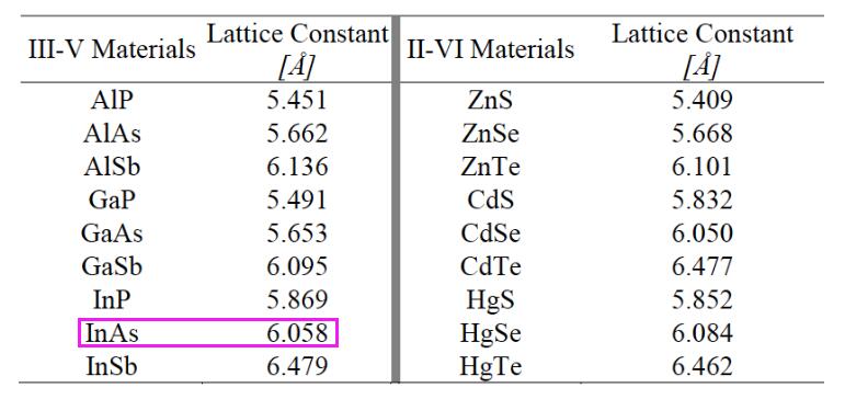
À partir du tableau de comparaison des constantes de réseau III-V et II-VI, la constante de réseau de l'arséniure d'indium est mise en évidence dans un cercle violet :
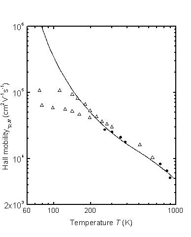
* Indium arsenide mobility and Hall effect
Sous différentes concentrations d'électrons, la relation entre la mobilité du hall d'électrons et la température est indiquée sur la figure :
* Indium arsenide transport properties in high electric fields
L'image suivante montre la dépendance du champ en régime permanent d'InAs :

* Recombination parameters of N type indium arsenide boule crystal
La durée de vie la plus longue des trous est τp ~ 3·10-6 s, et la longueur de diffusion Lp est d'environ Lp ~ 10 – 20 µm.
3. Application d'arséniure d'indium
Indium arsenide single crystal is used to make the infrared detector with a wavelength from 1 µm to 3.8 µm, high speed electronics, support communication and diode lasers. The emission wavelength of indium arsenide is 3.34μm, and lattice-matched In-GaAsSb, InAsPSb and InAsSb multi-epitaxial materials can be grown on the InAs substrate, which can manufacture lasers and detectors for optical fiber communication in the 2~4μm band.

Pour plus d'informations, veuillez nous contacter par e-mail à victorchan@powerwaywafer.com et powerwaymaterial@gmail.com.