
Plaquettes de phosphure d'indium : le matériau de base pour les interconnexions optiques à grande vitesse permettant la mise à l'échelle du calcul de l'IA +
PAM-XIAMEN can make InP epitaxial wafers for fabricating optical chips used in artificial intelligence (AI). More specifications please view the pages below, or contact our sales team at [email protected]
| Epitaxial Wafers | Diamètre | Wavelength Range | Applications |
| DFB Epitaxial Wafer | 2, 3, 4 inch | 1270 – 1654nm(Covering O, C, and L bands) | Optical communication (transmitter optical sub-assembly), LiDAR, gas sensing |
| EML Epitaxial wafer | 2, 3, 4 inch | 1310/1550/1577nm | Optical communication (transmitter optical sub-assembly) |
| DML plaquette épitaxiale | 2, 3, 4 inch | 1310/1342nm | Optical communication (transmitter optical sub-assembly) |
| FP Epitaxial wafer | 2, 3, 4 inch | 1310/1550nm | Optical communication (transmitter optical sub-assembly) |
| MPD Epitaxial wafer | 2, 3, 4 inch | 900-1650nm | Optical communication (transmitter optical sub-assembly) |
| APD Epitaxial wafer | 2, 3, 4 inch | 900-1650nm | Optical communication (receiver optical sub-assembly) |
| PIN Epitaxial wafer | 2, 3, 4 inch | 900-1650nm | Optical communication (receiver optical sub-assembly) |
With the rapid advancement of generative artificial intelligence and large-scale machine learning models, the parameter count of large language models has now surpassed the trillion scale. Training such models requires assembling tens of thousands to hundreds of thousands of GPUs, TPUs, or XPUs into massive computing clusters, within which the data communication throughput among processors grows exponentially. Figure 1 illustrates the computational power used for training representative AI systems in recent years, which has reached the petaFLOPs scale and is growing at a pace far exceeding Moore’s Law projections. This trend poses unprecedented challenges for short-reach optical interconnects (50m to 2km) linking processors: the per-lane data rate must evolve from the current 200Gbit/s toward 400 Gbit/s or beyond, and the total module capacity must rapidly scale from 800G and 1.6T to 3.2T.
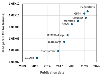
Fig. 1 Computational Power Used for AI Model Training
In communication links, optical interconnects, leveraging their advantages of high bandwidth, low latency, low power consumption, and immunity to electromagnetic interference, have become the critical infrastructure supporting the scaling of AI compute. Traditional pluggable optical modules have evolved from 400G to 800G and are rapidly advancing toward 1.6T. However, the fundamental bottleneck for achieving next-generation data rates is no longer solely the CMOS electronic chip, but rather the optical chip—specifically, the lasers serving as light sources and the modulators responsible for electro-optic conversion. Therefore, understanding the basic architecture of optical communication systems and the core role of optical chips is a prerequisite for analyzing the value of indium phosphide (InP) substrate materials.
1. Fundamentals of Optical Communication Systems and Optical Chips
1.1 Optical Communication System Architecture
An optical communication system uses optical signals as information carriers and optical fibers as the transmission medium, achieving long-distance information transmission through electro-optic conversion. At the transmitter side, electrical signals are converted into optical signals by laser chips; after transmission through the optical fiber, the optical signals are converted back into electrical signals by photodetector chips. This “electrical-optical-electrical” conversion chain forms the foundation of all optical modules. Within an AI data center, tens of thousands of such links operate in parallel, forming a large-scale optical interconnect network.
1.2 Optical Chips and III-V Compound Semiconductors
Optical chips are the core components enabling the conversion between optical and electrical signals, primarily including laser chips and photodetector chips. They are fabricated from III-V compound semiconductor materials (InP, GaAs, AlInGaAs, etc.) because III-V materials possess a direct bandgap, enabling efficient generation or absorption of light. Among these, InP and its lattice-matched quaternary materials (such as AlInGaAs, InGaAsP) cover the most critical O-band (1310nm) and C-band (1550nm) for optical communications, making them the dominant materials for long-distance, high-speed optical interconnects.
• Laser Chips: Integrating multiple epitaxial layers including the active region, waveguide layer, cladding layers, electrode contact layer, and PN junction, laser chips rely on quantum wells or quantum dots in the active region to convert electrical energy into optical energy and emit laser light. Their primary function is to convert electrical signals into optical signals, and they are the core component of the Transmitter Optical Sub-Assembly (TOSA).
• Photodetector Chips: Utilizing the photoelectric effect of semiconductor materials, photodetector chips convert optical signals back into electrical signals and are the core component of the Receiver Optical Sub-Assembly (ROSA).
The performance of optical modules—including data rate, power consumption, transmission distance, and reliability—is largely determined by these optical chips, whose performance in turn directly depends on the quality of InP substrates and the precision of their epitaxial structures.
2. InP Material Properties: Core Advantages and Positioning
2.1 Direct Bandgap and High-Efficiency Light Emission
Silicon (Si) and silicon nitride (SiN) offer low-loss passive optical waveguides, but their indirect bandgap nature precludes efficient light emission. InP, a III-V compound semiconductor, features a direct bandgap and exhibits extremely high electron-hole radiative recombination efficiency. By growing InP-based quantum well (QW) or quantum dot (QD) structures using metal-organic chemical vapor deposition (MOCVD) or molecular beam epitaxy (MBE), outstanding performance in communication bands can be achieved. Furthermore, InP-based QD lasers are insensitive to lattice-mismatch-induced defects, possess a high characteristic temperature, and can be directly integrated with silicon micro-ring modulators without optical isolators, thereby significantly reducing module power consumption and cost.
2.2 Mainstream Platform for Active Photonic Integration
The InP material system enables the realization of three major active functions—lasing, modulation, and detection—using the same epitaxial structure, a core advantage that distinguishes it from passive platforms such as silicon and silicon nitride. For example, the electro-absorption modulated laser (EML) integrates a distributed feedback (DFB) laser and an electro-absorption modulator (EAM) on a single chip, constituting the core device in optical modules operating at data rates of 200 Gbit/s per lane and above. Additionally, semi-insulating InP substrates (doped with Fe) provide excellent radio-frequency isolation, allowing the electro-optic bandwidth of modulators to exceed 100 GHz. It should be noted that silicon photonics platforms can also realize active functionality through heterogeneous integration (bonding or epitaxial growth of III-V materials) and offer greater cost advantages for large-scale passive optical network integration. InP’s advantage lies in the simplicity and maturity of monolithic integration, making it particularly suitable for light source and high-speed modulator applications that demand high reliability and performance.
3. Technical Requirements for InP Substrates and Epitaxy in AI Optical Interconnects
3.1 Data Rate Evolution and InP Device Bandwidth
The current mainstream 200 Gbit/s/lane PAM-4 transmission requires the electro-optic bandwidth of lasers/modulators to reach approximately 70 GHz. According to a review by Han et al., InP-based EMLs have already achieved a 93 GHz bandwidth and 420 Gbit/s PAM-8 transmission. For future 400 Gbit/s/lane, whether employing higher-order modulation or shifting to coherent detection, the demands on laser linewidth, relative intensity noise (RIN), and wavelength stability become even more stringent. For instance, dual-polarization 16QAM coherent transmission requires a laser linewidth below 500 kHz, which typically necessitates a long external cavity or high-quality InP/SiN heterogeneous integration.
3.2 Wavelength Division Multiplexing and Multi-Channel Integration
To increase per-fiber capacity, coarse wavelength division multiplexing (CWDM) and dense wavelength division multiplexing (DWDM) are widely adopted, resulting in an increase in the number of laser/modulator channels per optical module from 4 (for 400G) to 8 (for 800G/1.6T) or even more. The scaling of InP substrate size (transition from 4-inch to 6-inch) and on-wafer uniformity have become critical factors limiting manufacturability. The wavelength uniformity across an epitaxial wafer must be controlled within ±1 nm; otherwise, the insertion loss and crosstalk of the wavelength multiplexer will be directly impacted, degrading the overall link budget.
3.3 Extreme Requirements for Substrate Flatness in Heterogeneous Integration
To simultaneously leverage InP’s light source advantages and silicon photonics’ (SiPh) high-density passive integration capability, the industry is vigorously developing heterogeneous integration technologies. Researchers have detailed methods for transferring InP epitaxial films onto platforms such as silicon-on-insulator (SOI), silicon nitride (SiN), and even thin-film lithium niobate (TFLN) via direct wafer bonding or micro-transfer printing. This demands that InP substrates possess atomically flat surfaces, extremely low particulate contamination, and precisely controlled release layer structures.
4. Recent Technological Advances in InP Substrates and Epitaxy
4.1 Maturation of Quantum Well Lasers and Heterogeneous Integration
Conventional InP-based quantum well DFB/EMLs have reached a high degree of maturity and are commercially deployed at scale. Institutions such as Intel, IMEC, and NTT have fabricated complete optical transceivers on 300 mm Si wafers using heterogeneous bonding, achieving data rates of 256 Gbit/s OOK and 340 Gbit/s PAM-4. Furthermore, GaAs/InGaAs quantum well lasers grown directly on 300 mm CMOS production lines have demonstrated output powers exceeding 1 mW, threshold currents as low as 5 mA, and operation at temperatures up to 55 °C. These advances rely on large-diameter InP substrates and high-precision MOCVD epitaxy processes.
4.2 Quantum Dot Lasers: A Disruptive Light Source
Quantum dot structures are insensitive to dislocations, enabling direct epitaxial growth on silicon substrates without complex bonding processes. Han et al. reported electrically pumped quantum dot lasers on 300 mm Si wafers with output powers of 126.6 mW and operation up to 60 °C. Of even greater interest are quantum dot mode-locked lasers (QD MLLs), which can generate dozens of equally spaced optical frequency combs serving as multi-wavelength sources for DWDM. Such devices impose stricter requirements on lattice matching and surface defect density of InP substrates, but once engineering breakthroughs are achieved, they will enable truly monolithic silicon photonic integration.
4.3 Epitaxial Transfer Techniques in Heterogeneous Integration
Micro-transfer printing allows InP epitaxial structures to be “printed” from a source wafer onto a target photonic integrated circuit (PIC), avoiding the stress and alignment challenges associated with full-wafer bonding, while also enabling the hybrid integration of multiple material systems with different bandgaps. This technique has already realized monolithic integration of electrically pumped lasers and 50 GHz modulators on a TFLN platform, achieving a transmission rate of 128 Gbit/s OOK.
5. Market Supply and Demand: Super-Linear Growth in InP Demand
Selon la feuille de route d'Ethernet Alliance, la demande de modules optiques 1,6T et 3,2T dans les centres de données d'IA devrait connaître une croissance explosive entre 2025 et 2030. Un rapport de recherche de LightCounting estime que la taille du marché mondial des modules optiques Ethernet et des optiques co-packagées (CPO) utilisés dans les clusters d'IA atteindra 16,5 milliards en 2025 et atteindra 26 milliards en 2026, ce qui représente une augmentation d'environ 100 % d'une année sur l'autre. 60%. Dans la structure des coûts des modules optiques, les puces et composants optiques basés sur InP représentent environ 46,4 %, ce qui en fait le poste de coût le plus important. Par conséquent, la croissance des livraisons de modules optiques se traduit par une demande de substrats InP avec un effet de levier élevé. Mark&Spark Solutions prévoit que les ventes mondiales de plaquettes InP (équivalentes à 2 pouces) passeront d'environ 2,43 millions d'unités en 2024 à 7,31 millions d'unités d'ici 2032, ce qui représente un taux de croissance annuel composé (TCAC) de 14,76 %.
L'évolution continue du calcul de l'IA a fait des interconnexions optiques un goulot d'étranglement majeur dans l'ensemble du système informatique, tandis que les performances et le coût des interconnexions optiques dépendent fortement des substrats de phosphure d'indium et des plaquettes épitaxiales. InP est actuellement la plate-forme matérielle dominante capable de fournir simultanément une émission de lumière à haut rendement, une modulation et une détection à grande vitesse, occupant une position irremplaçable dans les puces laser (le cœur de TOSA) et les puces photodétecteurs (le cœur de ROSA).

Que vous ayez besoin d'une plaquette épitaxiale InP pour la recherche ou pour des applications industrielles, veuillez nous contacter par e-mail à[email protected]et[email protected].
Les références:
1. Ossieur, P., Moeneclaey, B., Coudyzer, G., Lambrecht, J., Craninckx, J., Martens, E., … & Bauwelinck, J. (2025). Photonique et électronique intégrées pour les émetteurs-récepteurs optiques prenant en charge les applications AI/ML. Journal IEEE de sujets sélectionnés en électronique quantique, 31(3), 1-16.
2. Han, C., Li, M., Guo, J. et Bowers, JE (2025). Technologies laser intégrées pour les applications d’intelligence artificielle. Optique Express, 33(23), 49431-49468.