IV Test Report
A test report is necessary to show the compliance between custom description and our final wafers data. We will test the wafer characerization by equipment before shipment, testing surface roughness by atomic force microscope, type by Roman spectra instrument, resistivity by non-contact resistivity testing equipment,micropipe density by polarizing microscope, orientation by X-ray Orientator etc. if the wafers meet the requirement, we will clean and pack them in 100 class clean room, if the wafers do not match the custom spec, we will take it off.
Testing Project: IV Test project
Current – voltage (IV) measurement is the basic electrical characteristic of device innovation.IV measurement is the task of obtaining current and voltage or resistance characteristics by providing voltage/current stimulation and measuring current/voltage responses. It is a fundamental electrical measurement and a fundamental method for discovering the behavior and characteristics of semiconductor chips.
See below example:
1.1 Test process:
(1) Cutting into 8×8×5mm3 wafers,4pcs;
(2) Lapping, polishing
(3) Etching:BrCHOH3
(4) Gelatinization, Development,Deposition,Stripping
(5) Passivation:H2O2
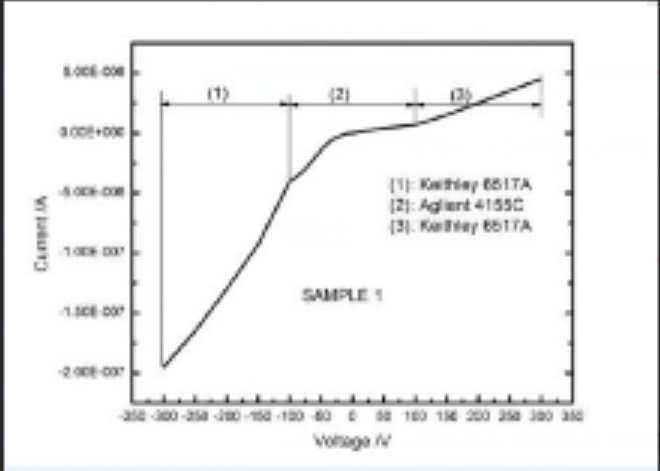
(6)Test:By Aglient 4155C in the range between-100V and By Keithley 6517A microgalvanometer above 100V.
1.2 Comments:
(1) chip electrode showed a greater asymmetry.
Below is an example of IV test of CZT:
For more information, please visit our website: https://www.powerwaywafer.com,
send us email at angel.ye@powerwaywafer.com or powerwaymaterial@gmail.com.

