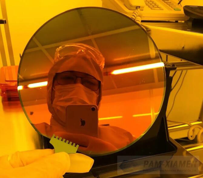
PAM-XIAMEN offers lapped silicon carbide wafers, As-cut wafers are lapped and cleaned to be qualified as lapped wafers. What is wafer lapping? Wafer lapping is a global flattening process that improves wafer flatness by removing surface damage (usually from back grinding). It is most commonly found in silicon carbide. Lapping is carried out between two reversed rotating cast iron plates and grinding film or slurry. To adjust the permeability of the film/paste, the wafer either spins faster or undergoes a heavier load to meet the target specification. Lapping wafer process can reduce surface roughness and mechanical defects from as-cut wafers and can further improve geometrical performance.
1. Specifications of Lapped Wafers
| 4″ 4H Silicon Carbide | |||||||
| Item No. | Type | Orientation | Thickness | Grade | Micropipe Density | Surface | Usable area |
| N-Type | |||||||
| S4H-100-N-SIC-370-L | 4″ 4H-N | 0°/4°±0.5° | 370±25um | D | * | L/L | >75% |
| 3″ 4H Silicon Carbide | |||||||
| Item No. | Type | Orientation | Thickness | Grade | Micropipe Density | Surface | Usable area |
| N-Type | |||||||
| S4H-76-N-SIC-370-L | 3″ 4H-N | 0°/4°±0.5° | 370±25um | D | * | L/L | >75% |
| 2″ 4H Silicon Carbide | |||||||
| Item No. | Type | Orientation | Thickness | Grade | Micropipe Density | Surface | Usable area |
| N-Type | |||||||
| S4H-51-N-SIC-370-L | 2″ 4H-N | 0°/4°±0.5° | 370±25um | D | * | L/L | >75% |
| 2″ 6H Silicon Carbide | |||||||
| Item No. | Type | Orientation | Thickness | Grade | Micropipe Density | Surface | Usable area |
| N-Type | |||||||
| S6H-51-N-SIC-370-L | 2″ 6H-N | 0°/4°±0.5° | 370±25um | D | * | L/L | >75% |
| SEMI-INSULATING |
| S6H-51-SI-SIC-370-L | 2″ 6H-SI | 0°/4°±0.5° | 370±25um | D | * | L/L | >75% |
2. Process of Lapped Wafers
The purpose of wafer lapping is to remove the knife marks on the surface of the SiC slice and the surface damage layer caused by the cutting process. Due to the high hardness of SiC wafer, a high-hardness abrasive (such as boron carbide or diamond powder) must be used to grind the crystal surface of the SiC slice during the lapping wafer process. Lapping can be divided into coarse lapping and fine lapping according to different processes.
2.1 Rough Lapping of SiC Wafer
Rough lapping is mainly to remove the knife marks caused by cutting and the deteriorated layer caused by cutting, and use abrasive grains with a larger particle size to improve processing efficiency.
2.2 Fine Lapping for Silicon Carbide Wafer
Fine lapping mainly removes the surface damage layer left by rough lapping, improves the SiC wafer surface finish, and controls the surface shape and the thickness of the silicon carbide wafer to facilitate subsequent polishing. Therefore, abrasive grains with finer particle diameters are used to grind the wafer.
Due to the low fracture toughness of silicon carbide, it is easy to crack during the lapping process, making the lapping of SiC wafers very difficult. Effective lapping requires the selection of appropriate lapping parameters to obtain the maximum material removal rate and control the surface integrity for lapped wafers.

For more information, please contact us email at victorchan@powerwaywafer.com and powerwaymaterial@gmail.com.