Single crystal germanium wafer with orientation (110) miscut toward <111> with 4 deg. or 12 deg. is provided without dopant. Due to the similar chemical properties with silicon, single crystal germanium has similar applications. While hall effect germanium wafer has higher sensitivity to gamma radiation, and is effective for detecting the applications of photo. Therefore, single crystal germanium wafer is the prime option for applications with high photodetction requirement, such as LEDs, fiber optics, solar cells and infrared optics. More about the Ge wafer (110) with miscut toward <111> please see below:
1. Specifications of Monocrystalline Ge with Miscut
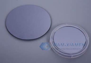
No.1 Single Crystalline Ge Wafer (PAMP21040)
4 inch Ge (110) wafer with 4 deg. off toward <111>
Undoped,
Thickness: 300±25um
Single side polished
No.2 Single-Crystal Ge Substrate (PAMP21256)
4 inch Ge (110), miscut toward <111> with 12 deg. wafer
Undoped,
Thickness: 300±25um
Single side polished
The crystal orientation of ‘(110) wafer with miscut toward <111>’ is same as below image:
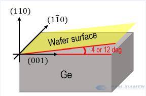
Single Crystal Germanium Wafer with Orientation (110) Miscut
2. Criterion – X-ray Diffraction Criterion for Detecting the Orientation of Single Crystal Germanium Wafer
The crystal orientation of the germanium single crystal wafer can be determined by the X-ray diffraction method. Specifically, when a beam of monochromatic X-ray with a wavelength of λ is incident on the surface of a germanium crystal, and the grazing angle θ between the main crystal plane of the crystal conforms to Bragg’s law, X-ray diffraction will occur. The counter is used to detect the diffraction line, and the main crystal orientation of the crystal can be determined according to the position of the diffraction line. The crystal orientation of germanium single crystal is determined by X-ray directional instrument. Generally, Ka radiation of copper target is used. After nickel filter, approximate monochromatic X-ray can be obtained with wavelength λ=0.154178nm. Bragg formula:
adsin θ =nλ (1)
In formula:
“θ” is Bragg angle (grazing angle), degrees (minutes);
“λ” stands for X-ray wavelength, λCuKa=0.154178nm;
“n” is an interference level, a positive integer;
“d” is the distance between diffracted crystal planes.
d=a/√h2+k2+l2 (2)
In formula:
“a” is the lattice constant, a=5.6575(Ge);
“h, k, l” represent crystal plane index (Miller index).
The incident X beam, the diffracted X beam and the normal of the diffraction surface are in the same plane, and the angle between the diffracted X beam and the transmitted X beam is 2θ.
When CuKd radiation is used as the incident X-beam (in=0.154178nm), the Bragg angle (grazing angle) that diffracts on the low-index crystal plane of germanium, showing as in the following table:
| Diffraction Angle | Bragg Angle θ | ||
| h | K | l | |
| 1 | 1 | 1 | 13°39’ |
| 2 | 2 | 0 | 22°40’ |
| 3 | 1 | 1 | 26°52’ |
| 4 | 0 | 0 | 33°02’ |
| 3 | 3 | 1 | 36°26’ |
| 4 | 2 | 2 | 41°52’ |

For more information, please contact us email at victorchan@powerwaywafer.com and powerwaymaterial@gmail.com.