Gallium oxide (Ga2O3) is a direct ultra wide bandgap semiconductor with a relatively complex structure. Ga2O3 has 5 isomers, namely α、β、γ、ε and δ. These five crystal phases can undergo phase transformation and mutual transformation under certain conditions, among which β- Ga2O3 is the most stable and common phase. Beta gallium oxide material is currently the most researched and the closest material to application in the semiconductor industry, and its industrialization is mainly focused on β-phase Ga2O3. PAM-XIAMEN is able to provide N-type and semi-insulating beta Ga2O3 substrates with the following specifications as a reference:
1. Specifications of Beta Ga2O3 Crystal Substrate
1.1 Semi-insulating Beta Ga2O3 Crystal Wafer
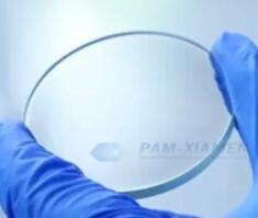
No. 1 50.8mm Ga2O3-β Wafer
PAM210730 – βGAO
| 2 Inch Beta Ga2O3 Substrate | ||
| Orientation | (-201) | |
| Dopant | Fe | |
| Conductivity | Semi-Insulating (>1010Ω.cm) | |
| Dimensions | A-B(mm) | 50.8±0.3 |
| C-D(mm) | 49.5±0.3 | |
| Thickness(mm) | 0.68±0.02 | |
| Offset angle(degree) | [010]: 0±1 | |
| [100]: -0.7±1 | ||
| FWHM(arcsec) | [010]: 150 or less | |
| [102]: 150 or less | ||
| Surface | Front | CMP |
| Back | Grinding | |
No.2 Ga2O3-β Single Crystal Substrate, <010>+/-1° ori, 1″x0.35mm, 2SP, Research grade with “Twin”
Substrate Specifications:
Chmistry: β-Ga2O3
Structure: Monoclinic
Lattice Constant: a=12.23A, b=3.04A, c=5.80A, ß=103.7°
Orientation: <010> +/-1°
Size: 1″ dia. x 0.35 mm
Conduction Type: Semi-insulating, Fe-doped
Doping density (Fe) : ~5E17 by SIMS.
Front surface finish: Epi-ready, RMS <0.5nm
Back surface finish: Optical polished
No.3 Ga2O3-β Single Crystal Substrate, <010>+/-1° ori, 10x10x0.35mm, 2SP, Research grade with “Twin”
Substrate Specifications:
Chmistry: β-Ga2O3
Structure: Monoclinic
Lattice Constant: a=12.23A, b=3.04A, c=5.80A, ß=103.7°
Orientation: <010> +/-1°
Size: 10×10 x 0.35 mm
Conduction Type: Semi-insulating, Fe-doped
Doping density (Fe) : ~5E17 by SIMS.
Front surface finish: Epi-ready, RMS <0.5nm
Back surface finish: Optical polished
No.4 Ga2O3-β Single Crystal Substrate, <010>+/-1° ori, 5 x 5 x 0.35mm, 2SP, Research grade with “Twin”
Substrate Specifications:
Chmistry: β-Ga2O3
Structure: Monoclinic
Lattice Constant: a=12.23A, b=3.04A, c=5.80A, ß=103.7°
Orientation: <010> +/-1°
Size: 5 x 5 x 0.35 mm
Conduction Type: Semi-insulating, Fe-doped
Doping density (Fe) : ~5E17 by SIMS.
Front surface finish: Epi-ready, RMS <0.5nm
Back surface finish: Optical polished
1.2 N Type β-Ga2O3 Wafer
No.1 50.8mm Beta Ga2O3 Substrate
PAM210730 – βGAO
| 2 Inch Beta Ga2O3 Substrate | ||
| Orientation | (001) | |
| Dopant | Sn | |
| Conductivity | n-type | |
| Nd-Na(cm-3) | 1×10¹⁸~2×10¹⁹ | |
| Dimensions | A-B(mm) | 50.8±0.3 |
| C-D(mm) | 49.5±0.3 | |
| Thickness(mm) | 0.65±0.02 | |
| Offset angle(degree) | [010]: 0±1 | |
| [100]: 0±1 | ||
| FWHM(arcsec) | [010]: 350 or less | |
| [100]: 350 or less | ||
| Surface | Front | CMP |
| Back | Grinding | |
No.2 Ga2O3-β Single Crystal Substrate, <100>+/-1° 10x10x0.75mm, 1SP
Substrate Specifications:
Chmistry: β-Ga2O3 ( Made in China)
Structure: Monoclinic
Lattice Constant: a=12.23A, b=3.04A, c=5.80A, ß=103.7°
Orientation: <100> +/-1° ( Please pay attention a, b, c axis defination above )
Type/Dopant: N type
Size: 10×10 x 0.7-0.8 mm
Polish: one side polished
Resistivity: <=0.2 ohm.cm
Surface roughness: < 5A
No. 3 Ga2O3-β Single Crystal Substrate, <-201> ori, 10x10x0.6mm, 1SP
Substrate Specifications:
Chmistry: β-Ga2O3 ( Made in China)
Structure: Monoclinic
Lattice Constant: a=12.23A, b=3.04A, c=5.80A, ß=103.7°
Orientation: <-201> +/-0.7° ( Please pay attention a, b, c axis defination above )
Type/Dopant: N type/Sn-doped
Size: 10×10 x 0.6 mm
Polish: one side polished
Surface roughness: < 5A
2. Properties of Beta Phase Gallium Oxide
In terms of electrical properties, the theoretical value of electron mobility of beta gallium oxide single crystal is 50 cm2/Vs, only 10-1 cm 2/Vs. The undoped β-Ga2O3 conductivity is relatively high with a magnitude of 109. Usually, doping is used to reduce the resistivity of thin films, such as doping with Sn to achieve n-type conductivity.
In terms of optical properties, β-Ga2O3 is a direct band gap semiconductor material, whose band gap corresponds to the optical absorption edge. Due to the large bandgap, the transparency is high in the deep ultraviolet (DUV) and visible light bands, with a transmittance of over 80% in the ultraviolet band. Usually, the luminescence types of beta Ga2O3 include three types:
1) ultraviolet light (3.2-3.6eV), which is generated by the combination of free electrons and self trapping holes;
2) Blue light (2.8~3.0eV) is generated by the recombination of donor level electrons and acceptor level holes;
3) Green light (2.4eV) is obtained by doping elements such as Be into Ga2O3.
In terms of gas sensitivity properties, the resistivity of β-Ga2O3 crystal is easily affected by the oxygen partial pressure in the environment, which changes with the oxygen partial pressure, making it sensitive to gas changes. Ga2O3-β material belongs to the anionic dense packing structure, which is prone to oxygen vacancies, and is sensitive to changes in gas concentration. It has good heat resistance and stable chemical properties, and can sensitively sense changes in oxygen concentration within the temperature range of 800 ℃ to 1000 ℃.
3. β-Ga2O3 for Wide-Bandgap Electronics and Optoelectronics
Due to its excellent structural properties, photoelectric properties, and gas sensitivity, β-Ga2O3 is widely used for various electronics and optoelectronics:
Semiconductor power devices: e.g. MOSFET;
High temperature gas sensor;
Transparent conductive film;
Sun blind ultraviolet detector and etc.
Additional Ga2O3 wafer specifications, please refer to:
GA2O3 BETA GALLIUM OXIDE WAFER AND CRYSTAL SUBSTRATES SEMI- INSULATING TYPE

For more information, please contact us email at victorchan@powerwaywafer.com and powerwaymaterial@gmail.com.