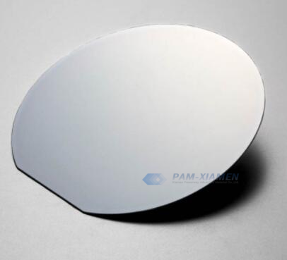
Semiconductor lasers in the near-infrared band (760-1060nm) based on GaAs substrates are the most mature and most widely used, and have already been commercialized. We can supply GaAs laser diode wafer for a wavelength of 940nm. Moreover, a variety of laser wafers with different wavelengths can be offered, more please refer to https://www.powerwaywafer.com/gaas-wafers/epi-wafer-for-laser-diode.
Theoretical and experimental studies have found that by adjusting the composition and thickness of each layer, the lasing wavelength of the InGaAs/AlGaAs quantum well laser can cover the range of 900-1300nm. This not only fills the gap of GaAs lasers and InP lasers in this band, but also greatly promotes the development of lasers and other related industries. More specification of GaAs laser diode epi wafer, please see table below:

1. 940nm InGaAs / GaAs Laser Diode Epitaxial Structure
|
940nm LD Structure (PAM201224-940LD) |
|||
| Material | Doping Concentration | Thickness | PL |
| P+ GaAs | P>5E19 | – | |
| P-AlGaAs | – | – | |
| Undoped AlGaAs | – | LOC~0.42um | |
| Undoped GaInAs active layer | – | – | 922+ -3nm |
| Undoped AlGaAs | – | – | |
| N-AlGaAs | – | d~2.5um | |
| N GaAs buffer | – | – | |
| N GaAs substrate, N=(0.4~4)x1018, d=350~625um, (100) 15° | |||
2. Why Use InGaAs/GaAs Material System to Fabricate Laser Diode?
In order to realize the GaAs laser diode wavelength of 940nm, since its transition energy is about 1.319eV, which is much smaller than the band gap of GaAs, the usual matching GaAs/AlGaAs (λ=0.7-0.9um) and InGaAsP/InP (λ=1.1-1.65um) is difficult to achieve. The emission wavelength of InGaAs material can be between 0.9-1.1um. However, none of the binary compounds have a substrate that matches its lattice. To grow on a GaAs substrate, a lattice mismatch of about 3% is required. If the epitaxial growth layer is thin enough, the stress due to the lattice mismatch can be withstand by the elastic deformation of the growth layer without producing defects or dislocations caused by excessive stress.
InGaAs/GaAs strained quantum well lasers do not suffer from sudden failures associated with dark line defects, and exhibit longer lifetimes than AlGaAs/GaAs semiconductor lasers. The <100> dark line defect has a high growth rate in GaAs quantum well lasers, but is suppressed in InGaAs quantum well lasers. The reason for this is that since In atoms are larger than Ga, Al, and As atoms, the propagation of defects is hindered and acts as a dislocation pinch-off agent. In addition, compared with the GaAs/AlGaAs laser, the energy released by the radiative and non-radiative recombination in the InGaAs quantum well laser is smaller; the InGaAs/GaAs interface has less non-radiative recombination centers than the AlGaAs/GaAs interface. The GaAs substrate is transparent to a wavelength of 940 nm, thereby reducing the rate of defect reactions due to recombination enhancement, such as diffusion, dissociation, and annihilation. So the InGaAs strain quantum well has better reliability for epitaxial gallium arsenide laser.
Because GaAs laser 940nmn adopts the important energy band engineering of semiconductor materials, not only the performance of semiconductor lasers has been further improved and improved, such as lower threshold current density, higher gain coefficient, and lower temperature sensitivity , more suitable for making high-power and long-life lasers, etc. Meanwhile, since the emission wavelength range of InGaAs/GaAs material system is 0.9-1.1um, it fills the emission wavelength blind area of matching GaAs/AlGaAs and InGaAsP/InP materials. Gallium arsenide semiconductor laser grown InGaAs as active layer has wider and more important application prospects in communication, medical and other fields.
Remark:
The Chinese government has announced new limits on the exportation of Gallium materials (such as GaAs, GaN, Ga2O3, GaP, InGaAs, and GaSb) and Germanium materials used to make semiconductor chips. Starting from August 1, 2023, exporting these materials is only allowed if we obtains a license from the Chinese Ministry of Commerce. Hope for your understanding and cooperation!
For more information, please contact us email at victorchan@powerwaywafer.com and powerwaymaterial@gmail.com.

