Actually, gallium oxide(Ga2O3) is not a new technology. Studies on gallium oxide applications in the field of power semiconductors are carried out by companies and research institutions all the time. And the gallium oxide material is mainly from Japan. With the development of Ga2O3 applications requirements becoming clearer, the performance requirements for high-power devices are getting higher and higher. Gallium oxide semiconductor has become the research hotspots and competition priorities in United States, Japan, Germany and other countries. PAM-XIAMEN has seen more deeply the advantages and prospects of gallium oxide semiconductor, and corresponding research has increased. At present, PAM-XIAEMN can offer Ga2O3 wafer in prime grade and dummy grade.
1. The Generational Change of Semiconductor Materials
First of all, we need to know the situation of each generation of semiconductors:
The first-generation semiconductor materials mainly refer to elemental semiconductor materials of silicon (Si) and germanium (Ge). The first generation of semiconductor materials, especially silicon, firmly occupies a dominant position in the development and application of semiconductor devices. It is the basis material for large-scale integrated circuits, analog ICs, sensors and other devices. Silicon processing technology is the cornerstone of the realization of Moore’s Law. Silicon-based chips have been widely used in computers, mobile phones, televisions, aerospace, and the new energy and silicon photovoltaic industries. As a result, many people outside the industry think that semiconductors are silicon when they mention semiconductors.
The second-generation semiconductor materials mainly refer to compound semiconductor materials, such as gallium arsenide (GaAs) and indium phosphide (InP), and also include ternary compound semiconductors, such as GaAsAl, GaAsP, and some solid solution semiconductors, such as Ge- Si, GaAs-GaP, glass semiconductors (also called amorphous semiconductors), amorphous silicon, glassy oxide semiconductors, organic semiconductors, like phthalocyanine, copper phthalocyanine, polyacrylonitrile, etc.
The third-generation semiconductor materials refer to wide-gap semiconductor materials, represented by silicon carbide (SiC), gallium nitride (GaN), and zinc oxide (ZnO). In terms of application, according to the development of third-generation semiconductors, its main applications are semiconductor lighting, power electronic devices, lasers and detectors, and the other four fields. Wide-bandgap semiconductors are still in the laboratory research and development stage.
The fourth-generation semiconductor materials are mainly ultra-wide band gap (UWBG) semiconductor materials, represented by diamond (C), gallium oxide (Ga2O3) semiconductor, and aluminum nitride (AlN), with a band gap exceeding 4eV, and ultra-narrow band gap (UNBG) semiconductor materials. Antimonide(GaSb, InSb) is the representative ultra-narrow band gap (UNBG) semiconductor material. In application, the ultra-wide Ga2O3 band gap material will overlap with the third-generation material, which mainly has more prominent characteristic advantages in the field of power devices; while due to easy excitation and high mobility of the ultra-narrow band gap material, it is mainly used for detectors and lasers.
2. The Characteristics of Gallium Oxide Semiconductor
Gallium oxide is an oxide of metallic gallium, and it is also a semiconductor compound. It has 5 confirmed crystalline forms, α, β, γ, δ, and ε. Up to now, among them, the β phase is the most stable. Take the gallium oxide semiconductor materials produced by PAM-XIAMEN as an example in the following part.
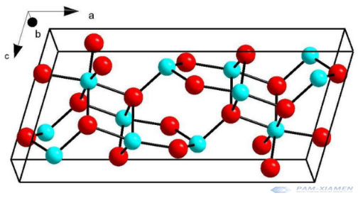
β-phase gallium oxide crystal structure
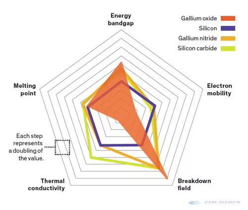
Most of the industry research reports related to the gallium oxide(Ga2O3) crystal growth and Ga2O3 properties in physics use β phase, and β phase is also widely used in domestic research and development. The β phase has a single Ga2O3 crystal structure called “β-gallia”. The band gap of the β phase is very large, reaching 4.8 to 4.9 eV, which is more than 4 times that of Si, and also exceeds the 3.3 eV of SiC and 3.4 eV of GaN (Table 1 is shown below). Under normal circumstances, the gallium oxide band gap is large, and the breakdown electric field strength will be large. The Ga2O3 breakdown field strength of the β phase is estimated to be about 8MV/cm, which is more than 20 times that of Si, which is equivalent to more than twice that of SiC and GaN. At present, research institutions have actually made 6.8MV/cm devices.
| Material | Bandgap/eV | Melting point/℃ | Electron mobility(cm2*V-1*s-1) | Electron saturation velocity/(107 cm*s-1) | Breakdown electric field/(108 V*m-1) | Dielectric constant | Thermal conductivity(W*cm-1*K-1) | Ballyga Merit |
| Si | 1.1 | 1410 | 1400 | 1 | 0.3 | 11.8 | 1.5 | 1 |
| GaAs | 1.4 | 1238 | 8000 | 2 | 0.4 | 12.9 | 0.55 | 5 |
| 4H-SiC | 3.3 | >2700 | 550 | 2 | 2.5 | 9.7 | 2.7 | 340 |
| GaN | 3.39 | 1700 | 600 | 2 | 3.3 | 9 | 2.1 | 870 |
| Diamond | 5.5 | 3800 | 2200 | 3 | 10 | 5.5 | 22 | 24664 |
| Gallium Oxide | 4.8-4.9 | 1740 | 300 | 2.42 | 8 | 10 | 0.27 | 3444 |
| Boron Nitride | 6 | >2937 | -1500 | 1.9 | -8 | 7.1 | 13 | 12224 |
While the β phase has excellent physical properties, it has low mobility and thermal conductivity, difficulty in manufacturing p-type semiconductors, which is inferior to SiC and GaN. However, current research shows that these aspects will not have much impact on the characteristics of power components, because the performance of power devices depends largely on the strength of the breakdown electric field. As for β-phase, the “Baliga’s figure of merit” as a low-loss indicator is proportional to the 3rd power of the breakdown electric field strength and proportional to the 1st power of the mobility.
The Baliga performance index was proposed by Mr. Jayant Baliga, who had been engaged in power semiconductor research and development for many years at General Electric in the United States. It is used for the performance evaluation of Unipolar Devices, like Power MOSFETs. There are “BFOM (Baliga`s Figure of Merits)”, which quantifies the theoretical loss of low frequency, and “BHFFOM (Baliga`s High Frequency Figure of Merits)”, which quantifies the theoretical loss of high frequency. In the field of power semiconductor R&D, low-frequency BFOM is widely used.
| Comparison of the characteristics of power semiconductor materials and components | ||||
| Silicon | 4H-SiC | GaN | β-Ga2O3 | |
| High voltage components | Mass production | Mass production | Under development | Research phase |
| Medium withstand voltage components | Mass production | Mass production | Mass production | Development stage |
| ON resistance of the element | Slightly higher | Low | Low | Very low |
| Low-frequency loss performance index(Relative value of BFOM) | 1 | 500 | 900 | 3,000(Very high) |
| Breakdown field strength (MV/cm) | 0.3 | 2.8 | 3.5 | 8(Estimated value) |
| Thermal conductivity (W/(cm*K)) | 1.5 | 4.9 | 2 | 0.1-0.3(low) |
| Substrate (wafer) cost | Extremely low | High | Very high (GaN substrate) | Low(Research stage) |
| Band Cap(Ev) | 1.1 | 3.3 | 3.4 | 4.8-4.9 |
| Vertical element | Mass production | Mass production | Under development(Slightly difficult) | Development phase(very likely) |
- β-Ga2O3 material is from Xiamen Powerway Advanced Material Co., Ltd.(PAM-XIAMEN)
Due to the high Balijia figure of merit of β-phase, when manufacturing unipolar power devices with the same withstand voltage, the on-resistance of the component is much lower than that of SiC or GaN. Experimental data shows that reducing the on-resistance is beneficial to reducing the power loss of the power circuit when it is turned on. Using β-phase power Ga2O3 devices can not only reduce the power loss during turn-on, but also reduce the loss during switching, because unipolar components can be used in high withstand voltage applications above 1kV. β-Ga2O3 is suitable for wide-bandgap electronics and optoelectronics.
For example, there is a unipolar transistor (MOSFET) that uses a protective film to reduce the concentration of the electric field to the gate, and its withstand voltage can reach 3k to 4kV. If silicon is used, a bipolar element must be used when the withstand voltage is 1kV. Even if SiC with a higher withstand voltage is used, a bipolar element must be used when the withstand voltage is 4kV. Bipolar devices use electrons and holes as carriers. Compared with unipolar devices that only use electrons as carriers, the generation and disappearance of carriers in the channel will be costly time during the on and off switching operations. The loss tends to be large.
In terms of gallium oxide thermal conductivity, if this parameter is low, it is difficult for power devices to work at high temperatures. However, the operating temperature in practical generally does not exceed 250°C, so there will be no effect on the operation in application. Since the heat-resistant temperature of packaging materials, wiring, solder, and sealing resin used in modules and power circuits encapsulated with power devices is no more than 250°C, the operating temperature of power devices should also be controlled below this level.
From another perspective, the easy-to-manufacture natural substrate, the control of carrier concentration, and the inherent thermal stability have also promoted the development of gallium oxide devices. Related papers expressed, when Ga2O3 substrate is doped N-type with Si or Sn, good controllability can be achieved.
Although some UWBG semiconductors (such as aluminum nitride AlN, cubic boron nitride c-BN and diamond) have more advantages than gallium oxide semiconductor in the BFOM chart, their material preparation and device processing are strictly limited. In other words, AlN, c-BN and diamond still lack technology accumulation for large-scale industrialization.
Comparison of the characteristics of key materials
Relevant statistics show that the loss of gallium oxide semiconductor is theoretically 1/3,000 of silicon, 1/6 of silicon carbide, and 1/3 of gallium nitride. In order to reduce the loss by 86%. People in the industry have high expectations for its future. And cost is another important factor to attract industry attention
The PVT method is commonly used in the production of SiC ingots. The solid SiC is heated to 2500°C for sublimation and then recrystallized on a high-quality SiC seed crystal with a slightly lower temperature. The core difficulties are:
1) The heating temperature is as high as 2500℃, and the SiC growth rate is very slow (<1mm/h);
2) The size of the grown crystal ingot is much shorter than that of Si;
3) The requirements for the seed crystal are very high, and it needs to have the characteristics of high quality and consistent with the required crystal diameter;
4) The hardness of SiC ingot is relatively high, and it is difficult to process and polish;
Based on SiC substrates, chemical vapor deposition (CVD) is commonly used to obtain high-quality epitaxial layers, and then power devices are fabricated on the epitaxial layers. The SiC substrate wafer has a higher defect density than Si, which will further interfere with the growth of the epitaxial layer. The epitaxial layer itself will also produce crystalline defects, which will affect the performance of subsequent devices.
Ga2O3, like sapphire, can be transformed from a solution state to a bulk (Bulk) single crystal state. In fact, by using the same guided mold method EFG (Edge-defined Film-fed Growth) as the sapphire wafer production technology, Japan NCT has tried to produce gallium oxide wafer with a maximum diameter of 6 inches (150 mm), and a diameter of 2 inches ( 50mm) wafers have been sold for research and development purposes. This process is characterized by high yield, low cost, fast growth rate, and large growth crystal size.
The “atomization method” used by Flosfia has produced 4-inch (100mm) α-phase Ga2O3 wafer, and the cost is close to that of silicon. But silicon carbide (SiC) and gallium nitride (GaN) materials can only be prepared by the “gas phase method” nowadays, and future costs will keep high owing to the high cost of the substrate. For gallium oxide semiconductor, compared with the current wide band gap SiC and GaN technologies, high-quality and large-size natural gallium oxide thin film will have unique and significant cost advantages.

3. Current Status of Research and Development and Industrialization of Gallium Oxide
Because it has so many advantages, gallium oxide is regarded as a technology with broader prospects than gallium nitride.
SiC or GaN. From the perspective of the division of labor in the industrial chain, Cree, Rohm, and ST have already formed a vertical supply system of SiC substrate → epitaxy → device → module. Manufacturers, such as Infineon, Bosch, OnSemi, etc., purchase substrates, then conduct Ga2O3 epitaxial growth by themselves and make devices and modules.
In terms of digital machines such as electric vehicles and “cheap” home appliances that have strict cost requirements, even if silicon carbide and gallium nitride have excellent performance, manufacturers can hardly accept their prices. Cost issues hinder the industry from adopting new semiconductor materials. FLOSFIA’s “Spray Drying Method” (MistDry) first dissolves gallium oxide in a solution mixed with dozens of formulas, and then sprays the solution on the sapphire substrate in a mist form. Gallium oxide crystals were formed before the solution on the sapphire substrate dries. In this way, the Ga2O3 thin film is obtained directly from the liquid state, without a high-temperature, ultra-clean environment, manufacturing of Ga2O3 wafer at a ultra low cost.
This kind of solution is liquid at room temperature, and the evaporation temperature does not need to reach 1,500 degrees, a few hundred degrees is enough; and the environment for making crystals is in room temperature air without any high-cost procedures. If small size is considered, it is possible that a semiconductor with the same price and better performance than silicon can be manufactured.
Due to material properties, some experts believe that gallium oxide semiconductor cannot be used to make P-type semiconductors. However, Shizuo Fujita of Kyoto University and Flosfia successfully developed a G2aO3 devices normally-off transistor (MOSFET) with a sapphire structure in 2016. Once gallium oxide material replaces the currently widely used silicon material, it will reduce 14.4 million tons of carbon dioxide emissions every year.
4. The Industry Characteristics of Power Semiconductors are Suitable for the Explosive Growth of Gallium Oxide Devices
Power semiconductors are used in all power electronics fields, and the market is mature and stable with slow growth. However, the industry always pursues higher power (faster charge and discharge), more efficient energy saving (reduced heat, safer and environmentally friendly), smaller size and weight (more portable and easier to install and maintain), and lower cost (broader Ga2O3 applications and markets). Therefore, in recent years, new application fields, such as new energy vehicles, renewable energy power generation, frequency conversion home appliances, and fast charging, have ushered in new huge growth.
①Industry feature 1: There is no need to catch up with Moore’s Law. Generally, 0.18~0.5um manufacturing process can be used. It relies on the quality of materials and has high requirements on the production process of materials and devices. Due to the overall trend toward integration and modularization, new packaging designs need to be developed .
Design procedure: The power semiconductor circuit has a simple structure and does not need to invest a lot of capital in architecture, IP, instruction set, design process, software tools, etc.
Manufacturing: Because there is no need to catch up with Moore’s Law, the production line is not highly dependent on advanced equipment, and the overall capital expenditure is small.
Packaging: It can be divided into discrete device packaging and module packaging. Because power devices have very high reliability requirements, special designs and materials are required, and the value of subsequent processing accounts for more than 35%, which is much higher than 10% of ordinary digital logic chips. At present, according to the research projects and product layout, many enterprises are beginning to transform to mid-to-high-end products with higher value .
②Industry feature 1: The power semiconductor industry generally adopts IDM mode, which is more suitable for enterprises to become bigger and stronger. Although the substrate and epitaxy companies can become separate part, and the chip design and manufacturing procedures must be integrated, otherwise the ability to make technological progress will be lost and the production capacity will be limited. Therefore, outsourcing can only be used as a supplement to the production capacity of low-end products.
③Industry feature 2: New energy vehicles and other emerging applications continue to promote the rise of new semiconductor materials.
The fourth-generation materials have the potential to cooperate with third-generation semiconductors to replace silicon materials in high-power and high-frequency application scenarios. The whole industry is in the initial stage of industrialization.
Driven by emerging market demands, like new energy vehicles, 5G, fast charging, and potential silicon replacement markets, the current in-depth research and industrialization are mainly based on SiC and GaN. Ga2O3 technical reserve is weak, so companies with such a technology face less competitive pressure.
The core difficulty of the fourth-generation semiconductor – gallium oxide semiconductor lies in the preparation of materials. Breakthroughs on the material side will gain great market value.
For more information, please contact us email at victorchan@powerwaywafer.com and powerwaymaterial@gmail.com.