GaN epi layers are usually grown by MOCVD on various substrates, such as sapphire, Si and SiC substrate. The choice of substrate varies according to the needs of the applications. So for RF MOSFET (Metal Oxide Semiconductor Field Effect Transistor) application, SiC substrate, which can provide the highest power levels of GaN wafers, with other outstanding features to ensure their use in the most demanding environments, is the preferred material for GaN hoteroepitaxial growth. Below listed SiC based GaN MOSFET structure is grown for RF applications. Besides, we can grow custom epitaxial GaN transistor structure for RF devices.

1. GaN MOSFET Structure Epitaxy on SiC Substrate for RF Applications
PAM200409-MOSFET
No.1 AlGaN / GaN MOSFET Structure
|
4-inch GaN on SiC Epi-Wafer (MOCVD) |
||||
| Layer Name | Material | Thickness (À) | Dopant | Concentration (cm-3) |
| 4. Cap | SiN | 60 | – | – |
| 3. Barrier | AlN | – | N/A | N/A |
| 2. Buffer | GaN Channel | – | – | – |
| AlGaN buffer | ||||
| 1. Nucleation | Nucleation | Standard | ||
| SiC substrate | ||||
No.2 GaN on SiC wafers with EPI structures for RF MOSFET
| 4-inch GaN on SiC Epi-Wafer (MOCVD) | ||||
| Layer Name | Material | Thickness (À) | Dopant | Concentration (cm-3) |
| 5. Cap | GaN | – | UID | – |
| 4. Barrier | Al0.25Ga0.75N | – | N/A | N/A |
| 3. Spacer | AlN | 8 | N/A | N/A |
| 2. Buffer | GaN Channel | – | Fe dope away from channel | |
| GaN buffer | ||||
| 1. Nucleation | Nucleation | Standard | ||
| SiC substrate | ||||
For the internal space of mobile phones, GaN on SiC epi structure can achieve good power consumption control. In satellite communications with high frequency and high power output requirements, it estimates that gallium nitride (GaN) technology will gradually replace GaAs and Si as a new solution since the GaN MOSFET advantages.
Among them, GaN-on-SiC MOSFET wafer combines the excellent thermal conductivity of SiC with the high power density and low loss capabilities of GaN. Compared to Si, SiC is a very dissipative substrate, making devices operate at high voltages and high drain currents, the junction temperature will slowly increase with RF power, resulting in better RF performance and a suitable material for RF applications.
2. Why Is GaN-on-SiC MOSFET Wafer Superior to Other Semiconductors in RF Market?
GaN-on-SiC MOSFETs are expected to replace the dominance of silicon-based LDMOS in the RF market in the near future. And GaN on SiC epi wafer stands out in RF applications for the following reasons:
GaN has a high breakdown electric field due to its large band gap, which allows GaN devices to operate at much higher voltages than other semiconductor devices. When subjected to a high enough electric field, electrons in a semiconductor can gain enough kinetic energy to break chemical bonds (a process known as impact ionization or voltage breakdown). If impact ionization is not controlled, device performance may be degraded. Since GaN devices can operate at higher voltages, they can be used in higher power applications.
Electrons on GaN have a very high saturation velocity (electron velocity at extremely high electric fields). When combined with the large charge capability, GaN MOSFETs on SiC substrates are able to deliver much higher current densities.
RF power output is the product of voltage and current swing, so the higher the voltage and the higher the current density, the more RF power can be produced in a life-size transistor. In short, devices fabricated on vertical GaN MOSFETs produce much higher power densities.
GaN-on-SiC devices exhibit unusual thermal properties, mainly due to the high thermal conductivity of SiC. Specifically, the temperature of device on GaN MOSFET structure does not become as high as a GaAs or Si device for the same power consumption. The lower the device temperature, the more reliable it is.
3. About MOSFET
The MOSFET is a type of IGFET (Insulated-Gate Field Effect Transistor) fabricated by controlled oxidation of a semiconductor. It is a field effect transistor that can be widely used in analog circuits and digital circuits. According to the polarity of the channel (working carrier), MOSFET can be divided into N-type and P-type, which is also known as NMOSFET (NMOS) and PMOSFET (PMOS). For GaN MOSFET vs Si MOSFET, GaN MOSFET can switch faster than that of silicon, and the slew rate of dV/dt is over 100 V/nsec.
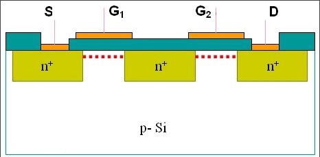
There are many common MOSFET technologies, such as dual-gate MOSFET, depletion mode MOSFET, power MOSFET, double-diffused MOSFET and so on. Among all the types, dual-gate MOSFET is usually used in RF integrated circuits. Both gates of this MOSFET can control the amount of current. In RF circuit applications, the second gate of a dual-gate MOSFET is mostly used for gain, mixer or frequency conversion control.

Typical Dual-Gate MOSFET Structure on Si Substrate
For more information, please contact us email at victorchan@powerwaywafer.com and powerwaymaterial@gmail.com.

