


GaP Wafer – Can’t Offer Temporarily
- Description
Product Description
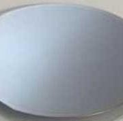
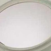
PAM-XIAMEN offers Compound Semiconductor GaP wafer – gallium phosphide wafer which are grown by LEC(Liquid Encapsulated Czochralski) as epi-ready or mechanical grade with n type, p type or semi-insulating in different orientation(111) or (100).
Gallium phosphide (GaP), a phosphide of gallium, is a compound semiconductor material with an indirect band gap of 2.26eV(300K). The polycrystalline material has the appearance of pale orange pieces. Undoped single gallium phosphide crystal wafers appear clear orange, but strongly doped wafers appear darker due to free-carrier absorption. It is odorless and insoluble in water. Gallium phosphide wafers by doping sulfur or tellurium can produce n-type semiconductors. Zinc is used as a dopant for the p-type semiconductor. Gallium phosphide wafer has applications in optical systems. Its refractive index is between 4.30 at 262 nm (UV), 3.45 at 550 nm (green) and 3.19 at 840 nm (IR). Gallium phosphide single crystal is the main substrate material for the preparation of red, green, yellow and orange visible light LEDs.
| Specs of GaP Wafer and Substrate | |
| Conducion Type | N-type |
| Dopant | S doped |
| Wafer Diameter | 50.8+/-0.5mm |
| Crystal Orientation | (111)+/-0.5° |
| Flat orientation | 111 |
| Flat length | 17.5+/-2mm |
| Carrier Concentration | (2-7)x10^7/cm3 |
| Resistivity at RT | 0.05-0.4ohm.cm |
| Mobility | >100cm²/V.sec |
| Etch Pit Density | <3*10^5/cm² |
| Laser Marking | upon request |
| Suface Fnish | P/E |
| Thickness | 250+/-20um |
| Epi Ready | Yes |
| Package | Single wafer container or cassette |
The Chinese government has announced new limits on the exportation of Gallium materials (such as GaAs, GaN, Ga2O3, GaP, InGaAs, and GaSb) and Germanium materials used to make semiconductor chips. Starting from August 1, 2023, exporting these materials is only allowed if we obtains a license from the Chinese Ministry of Commerce. Hope for your understanding and cooperation!
You may also like…
-
GaAs Epiwafer
PAM-XIAMEN is manufacturing various types of epi wafer III-V silicon doped n-type semiconductor materials based on Ga, Al, In, As and P grown by MBE or MOCVD. We supply custom GaAs epiwafer structures to meet customer specifications, please contact us for more information.
-
GaSb Wafer
PAM-XIAMEN offers Compound Semiconductor GaSb wafer – gallium antimonide which are grown by LEC(Liquid Encapsulated Czochralski) as epi-ready or mechanical grade with n type, p type or semi-insulating in different orientation(111) or (100).
-
Ge(Germanium) Single Crystals and Wafers
PAM-XIAMEN offers 2”, 3”, 4” and 6” germanium wafer, which is short for Ge wafer grown by VGF / LEC. Lightly doped P and N type Germanium wafer can be also used for Hall effect experiment. At room temperature, crystalline germanium is brittle and has little plasticity. Germanium has semiconductor properties. High-purity germanium is doped with trivalent elements (such as indium, gallium, boron) to obtain P-type germanium semiconductors; and pentavalent elements (such as antimony, arsenic, and phosphorus) are doped to obtain N-type germanium semiconductors. Germanium has good semiconductor properties, such as high electron mobility and high hole mobility. -
InP wafer
PAM-XIAMEN offers VGF InP(Indium Phosphide) wafer with prime or test grade including low dope, N type or semi-insulating. The mobility of InP wafer is different in different type, low doped one>=3000cm2/V.s, N type>1000 or 2000cm2V.s(depends on different doping concentration), P type: 60+/-10 or 80+/-10cm2/V.s(depends on different Zn doping concentration), and semi-insulting one>2000cm2/V.s, the EPD of Indium Phosphide is below 500/cm2 normally.
-
SiC Epitaxy
We provide custom thin film (silicon carbide)SiC epitaxy on 6H or 4H substrates for the development of silicon carbide devices. SiC epi wafer is mainly used for Schottky diodes, metal-oxide semiconductor field-effect transistors, junction field effect -
InSb wafer
PAM-XIAMEN offers Compound Semiconductor InSb wafer – Indium antimonide wafer which is grown by LEC(Liquid Encapsulated Czochralski) as epi-ready or mechanical grade with n type, p type or semi-insulating in different orientation(111) or (100). Indium antimonide doped with isoelectronic(such as N doping) can reduce the defect density during the indium antimonide thin films manufacturing process.
-
InAs wafer
PAM-XIAMEN offers Compound Semiconductor InAs wafer – indium arsenide wafer which are grown by LEC(Liquid Encapsulated Czochralski) as epi-ready or mechanical grade with n type, p type or semi-insulating in different orientation(111) or (100). In addition, InAs single crystal has high electron mobility and is an ideal material for making Hall devices.
-
GaN Templates
PAM-XIAMEN’s Template Products consist of crystalline layers of (gallium nitride)GaN templates, (aluminum nitride)AlN template,(aluminum gallium nitride) AlGaN templates and (indium gallium nitride) InGaN templates, which are deposited on sapphire


