Xiamen Powerway Advanced Material Co.,Ltd. offers monocrystal or polycrystalline150mm Germanium (100) or (111) substrates for optical application or for epi-growth in microelectronics. You can buy germanium substrate in following specifications:
1. Gemanium Substrate Specifications
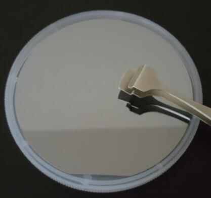
No.1 Optically Polished Germanium Substrates
PAM211025-GE
| Sl No’ | Specifications | Value |
| 1 | Material | Germanium (Ge) Optical grade |
| 2 | Crystalline form | Polycrystalline / Monocrystalline |
| 3 | Shape | Circular Flat |
| 4 | Diameter | 25 mm +0.0 / -0.10 mm |
| 5 | Thickness | 2 mm +/- 0.10 mm |
| 6 | Edge chamfer | 0.3 (+/- 0.1) mm x 45 degrees |
| 7 | Wedge | < 0.05 mm |
| 8 | Surface Quality (Scratch – Dig) | Both surfaces optically polished (60 – 40) |
| 9 | Clear Aperture (CA) | > 22 mm |
| 10 | Surface flatness | < 2 fringes (1 wave) over CA |
| 11 | Surface micro-roughness | < 3 nm |
| 12 | Conductivity type | n -type |
| 13 | Typical Resistivity | < 10 ohm-cm |
| 14 | Absorption coefficient at 25o C | < 0.04 cm-1 @10.6 mm |
| 15 | Refractive index @10.6 mm | 4.01 +/- 0.005 |
| 16 | Spectral Transmission in 3-11 mm | Greater than 45 %. |
No.2 Ge Substrate for Optics
Optical Grade PAM-190709-GE
Diameter: 6”dia.
(100) +/-0.5deg.
Thickness:2000±25µm,
Both-sides-polished
No.3 Germanium Wafer, undoped
Prime Grade PAM-190725-GE
Diameter: 6”dia.
Intrinsic undoped Ge,
(100) or (111)+/-0.5deg.
Resistivity>30 Ohm.cm,
Thickness:500±25µm,
SEMI Standard
TTV<5µm
Both-sides-polished,
Sealed in Empak or equivalent cassette.
No.4 Epi-ready Germanium Substrate, p type
Prime Grade PAM-190711-GE
Diameter: 6”dia.
P type/Ga doped,
(100) +/-0.5deg.
Resistivity: (0.005~0.05) Ohm.cm,
Thickness:500±25µm,
SEMI Standard
Single-sides-polished,
Sealed in Empak or equivalent cassette.
The epi-ready Germanium wafers also can be used for x-Ray diffraction after they are processed for a MEMS application. The Ge substrate can be DSP, undoped material, and minimum possible EPD for the final x-Ray application.
No.5 Polycrystalline Germanium Substrate PAM190709-GE
Purity:>=99.999%
N type
Size:60mm x 8mm
Thickness:1000um
Double side polished
No. 6 Optical Ge Wafer PAM200528-GE
Purity: 99.999%
Orientation: <100>,<110>,<111> (accuracy < 1°)
Dia.50.8mm (+/- 0.5mm)
Thichness 1.5mm
- The light ring of germanium spec is 10, and effective aperture is 85%.
2. Advantages of Germanium Substrate During Process
The main advantages of germanium sheet processing are as follows:
The germanium single crystal multi-wire cutting process has the characteristics of low material loss and high geometric parameters of the cutting slice;
The back grinding and weak corrosion technology not only improves the mechanical strength of the germanium slice, but also maintains the surface state of the ground surface;
At the same time, it can also achieve the purpose of eliminating the internal stress introduced by grinding, controlling the roughness of the corroded surface and cleaning the grinding surface of the germanium plate;
The three-step polishing process technology of germanium substrate realizes the effect of balancing the chemical and mechanical effects in the polishing process, so that the ultra-thin germanium slices after polishing can achieve better geometric parameter accuracy and surface roughness;
The unique cleaning and packaging process can improve the shelf life of germanium wafer.
3. Single Crystal Germanium Substrate Industry Standards
According to the conductivity type, single crystal germanium material is divided into N type and P type.
3.1 Designation Method of Germanium Substrate
The “1” indicate the production method of germanium wafers, use CZ for Czochralski method, and HB for horizontal method.
The “2-Ge” stands for crystal germanium wafer.
The “3” uses N or P to indicate the conductivity type, and the element symbols in parentheses indicate dopants.
The “4” uses Miller index to indicate crystal orientation.
Examples of Ge Substrate Designation:
a) CZ-Ge-n(Sb)-<111>indicates that the crystal orientation is <111> N-type antimony-doped Czochralski single crystal germaniumsubstrates.
b) CZ-Ge-p(Gn)-<111>indicates that the crystal orientation is <111>P-type arsenic-doped Czochralski germanium wafers.
3.2 The specifications of the germanium substrate meet the requirements in the table:
| Item | Geometry parameters/ mm | |
| Square wafer | Corrosion wafer | |
| Side length | 0.90×0.90 | 0.85×0.85 |
| 1.00×1.0O | 0.90×0.90 | |
| 2.00×2.00 | 0.95×0.95 | |
| 2.25×2.25 | – | |
| Allowable deviation of side length | ± 0.05 | ± 0.05 |
| Thickness | 0.24~0.30 | 0.13~0.17 |
| Thickness tolerance | ± 0.01 | ± 0.01 |
3.3 Germanium Substrate Surface Quality
3.3.1 Surface Quality Inspection of Optical Germanium
We inspect the optical grade germanium substrate for scratches by strong light (Multi-angle parallel light source) in a dark room.
Inspection Purpose: To determine whether there are fine scratches, foreign bodies, microbubbles on the optic germanium surface.
Inspection Content: Inspect for fine scratch on Ge substrate surface
Reference Light Source: Multi-angle parallel light source
Analysis: The inspection for fine scratch, foreign matter on glass surface.
The glass is a highly reflective object, and the multi-angle parallel light source can illuminate the fine scratches clearly, and very uniform.
Scratch/Dig: 60/40 means:
60: max allowable scratch width (0.06mm width)
40: max allowable dig diameter (0.4mm diameter)
More about the scratch or dig number, please refer to the table below:
| Scratch Number | Maximum Allowable Scratch Width (mm) |
Dig Number | Maximum Allowable Dig or Bubble Diameter (mm) |
|
| 120 | 0.12 | 120 | 1.2 | |
| 80 | 0.08 | 80 | 0.8 | |
| 60 | 0.06 | 60 | 0.6 | |
| 50 | 0.05 | 50 | 0.5 | |
| 40 | 0.04 | 40 | 0.4 | |
| 30 | 0.03 | 30 | 0.3 | |
| 20 | 0.02 | 20 | 0.2 | |
| Purpose: glass surface quality on optical components Definitions: Procedure: |
||||
3.3.2 Surface Quality Inspection of Epi-ready Germanium
a) Germanium single crystal square substrates must not have a chipped edge with a length greater than one-seventh of the side length, and a Ge wafer with a side length not greater than 2mm. The width of the chipped edge shall not exceed one-tenth of the side length. For germanium substrates with a side length greater than 2mm, the width of chipping shall not exceed one twentieth of the side length, and the number of chippings for each chip shall not be more than 2.
b) The thin germanium wafer is not allowed to have cracks.
c) After the single crystal germanium sheet is washed and dried by ultrasonic, the surface should be cleaned without stains.
d) The germanium cutting disc shall not have obvious knife marks.
e) There should be no scratches and knife marks on the surface of the germanium abrasive sheet.
f) The surface of the germanium corroded sheet should be free of scratches, knife marks, stains, dirt and lamination.
3.4 Testing method for Germanium Substrate
a)The conductivity type is determined in accordance with GB/T 1550.
b)The measurement of resistivity is carried out in accordance with the GB/T1552.
c)The measurement of Ge substrate dislocation density shall be carried out in accordance with the GB/T 5252.
d)The determination of crystal orientation shall be carried out in accordance with the GB/T 5254.
e)The life of a few collectors should be measured in accordance with GB/T 1553.
f)The measurement of geometric parameters is divided into:
- The side length of the germanium single crystal square piece is measured with a 0.01mm micrometer or a measuring tool with equivalent accuracy;
- The thickness of the Ge substrates is measured with a dial indicator with an index of 0.001mm or a measuring tool with equivalent accuracy.
g)The inspection of surface quality shall be carried out by visual inspection.

For more information, please contact us email at victorchan@powerwaywafer.com and powerwaymaterial@gmail.com.