Monocrystalline silicon is widely used in microelectronic applications due to its low cost, mature manufacturing process, high carrier mobility, and long-term stability. And the growing silicon wafers applied in optoelectronic applications, such as photodetector, takes up a small portion. Monocrystalline silicon has a good response to light in the 850nm wavelength range, making it an ideal photosensitive material for bulk silicon photodetectors in the 500nm-1000nm wavelength range. PAM-XIAMEN is growing silicon wafers for your device fabrication. Attached are the specific parameters of Si wafer for photodetctor for your information:
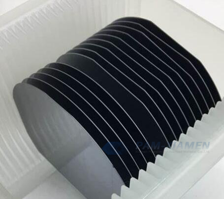
1. Growing Silicon Wafers for Photodetector (PAM200928 – SI)
No. 1 P-Type, B-Doped Silicon Wafer
| Item | Si wafer |
| Diameter | 76mm (3inch) |
| Orientation | (111), 0 +/-2⁰ |
| OF orientation | (110), 0+/-3⁰ |
| Type | p-type, B-doped |
| Thickness | 600+30-60 um |
| TTV | <= 12um |
| Surface finished | Double side polished |
| Front side | Rz <= 0.050 |
| Back side | Rz <= 0.050 |
| Dislocation density | <=1*101 cm-2 |
| Minority carrier lifetime | >= 500us |
| Resistivity | 7000-15000 Ohm*cm |
| Resistivity spread | +/-20% |
| Scratches quantity (length <= 400um, width <= 10um) | <= 5pcs |
| Quantity of light points (in the dark field of the microscope, at a magnification of 200x) | <= 9pcs |
| Chips quantity (along the perimeter of the wafer outside the working area, chips size <= 1mm) | <= 5pcs |
| Working area diameter | 70mm |
No. 2 N-Type, P-Doped Silicon Substrate
| Item | Si wafer |
| Diameter | 76mm (3inch) |
| Orientation | (111), 0 +/-2⁰ |
| OF orientation | (110), 0+/-3⁰ |
| Type | n-type, P-doped |
| Thickness | 400 +/-20 um |
| TTV | <= 12um |
| Surface finished | Double side polished |
| Front side | Rz <= 0.050 |
| Back side | Rz <= 0.050 |
| Dislocation density | <=1*101 cm-2 |
| Minority carrier lifetime | >= 100us |
| Resistivity | 150-200 Ohm*cm |
| Resistivity spread | +/-20% |
| Scratches quantity (length <= 400um, width <= 10um) | <= 5pcs |
| Quantity of light points (in the dark field of the microscope, at a magnification of 200x) | <= 9pcs |
| Chips quantity (along the perimeter of the wafer outside the working area, chips size <= 1mm) | <= 5pcs |
| Chips, gouges and undercuts are allowed at a distance of no more than 2-3 mm from the edge | |
Silicon Wafer Growth: manufactured by the crucible-free method from polycrystalline silicon obtained by hydrogen reduction of chlorosilanes, thermal decomposition of monosilane
2. About Bulk Silicon based Photodetectors
For bulk silicon based photodetctor, there are two type structures of the photodetector grown on bulk silicon:
1) Vertical Si PIN detector: The responsiveness and response speed of vertical structure silicon PIN detectors will be mutually constrained. To achieve high responsiveness, it is necessary to have a long light absorption length, which means there should be growing silicon wafers with a thick low doping layer between the p-type and n-type layers. This will increase the transit time of photo generated carriers and decrease the response speed of the device. If this constraint is not lifted, it will be difficult to produce high-speed and appropriately responsive silicon-based PDs.
2) Horizantal Si PIN detector: The PIN detector with a horizontal structure makes the propagation direction of light perpendicular to the movement direction of photo generated charge carriers, thereby controlling the absorption length of light and the transition length of photo generated charge carriers, respectively.
To improve the speed of silicon photodetectors, we can relieve the constraints on the quantum efficiency and response speed of the detector, create a silicon surface with microstructure, and utilize the total internal reflection of light at the microstructured silicon surface to increase light absorption.
Create a resonant cavity enhancement structure, which involves placing the light absorbing responsive medium material in a Fabry Perot cavity. Light that meets the resonance conditions will resonate in the cavity and be enhanced and absorbed by resonance. In this way, even thinner light absorbing materials can achieve higher quantum efficiency.
3. Development of Si-based Long Wavelength Photodetectorsfor Optical Communication & Interconnection
Silicon wafers for chips become transparent at wavelengths greater than 1100nm and loses its detection ability, as shown in the following figure (The relationship among the light absorption coefficient of Si and the wavelength and depth of light penetration). Moreover, the low movement rate of charge carriers in silicon wafer production makes it difficult for devices to achieve high-speed reactions. Therefore, in response to these issues faced by silicon based detectors used for optical communication and optical interconnection.
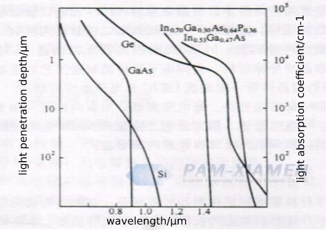
The relationship among the wavelength of Si and the light absorption coefficient and the light penetration depth
The research work for growing silicon photodetector for optical communication and interconnection at home and abroad mainly focuses on:
1) Designing novel structures to improve the performance of devices (quantum efficiency, rate, noise) and implementing special applications (such as dense wavelength division multiplexing (DWDM);
2) Epitaxing other materials on silicon wafer to achieve long wavelength detection, currently the main epitaxial material used is germanium, which is a Ge-on-Si detector.

For more information, please contact us email at victorchan@powerwaywafer.com and powerwaymaterial@gmail.com.