HEMTs evolved from Field Effect Transistors (FETs) are suitable for manufacturing monolithic microwave integrated circuits (MMICs).
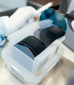
HEMTs were initially generated to obtain high electron mobility in semiconductor devices at room temperature. The electron mobility of FETs is limited even with high doping levels, so high electron mobility obtained with AlxGa1-xAs/GaAs quantum well HEMTs heterostructures with has rapidly replaced metal-semiconductor FETs (MESFETs) in wireless communication circuits. PAM-XIAMEN can offer AlGaAs/GaAs HEMT epiwafer, more please view: https://www.powerwaywafer.com/gaas-hemt-epi-wafer.html.
1. About HEMT Techonology
The high electron mobility in HEMT structure results from the combination of doped wide band semiconductor and undoped narrow band gap semiconductor. The structure of the two materials with different band gaps forms a heterojunction with the doping zone of the channel. Such HEMT are also known as heterostructure FET (HFET) or modulation doped FET (MODFET).
GaN / AlGaN HEMT technology is developing rapidly, making HEMT devices suitable for high voltage, high current and low on-resistance circuits. Different from Si or GaAs based devices, devices fabricated on GaN HEMT wafer have special propertities of higher breakdown voltage, saturation electron drift velocity, thermal conductivity and power dissipation density. GaN HEMT epitaxial wafer can be supplied, details please read https://www.powerwaywafer.com/gan-wafer/gan-hemt-epitaxial-wafer.html.
When two types of semiconductor with different band gap and doping levels are integrated into the device structure, electrons move towards the narrow-bandgap material with lower energy. This charge transfer is repelled by the electric field between the electron and the donor ion, tending to change the charged potential.
The carriers are confined to the triangular quantum well region of the narrow gap undoped material, which is adjacent to the wide gap doped material. The thinness of the quantum well region produces 2DEG of the free carrier.
In this 2DEG, there are no other donor electrons. Thus, the electron mobility in this region is very high. This heterostructure is conducive to high electron mobility in HEMTs.
Using two semiconductors in the HEMT structure have the same lattice constant or atomic spacing. If the lattice constants do not match, it can result in band discontinuities, deep traps, and ultimately HEMT performance degradation.
Only a few electrons are confined in the channel due to the slight conduction band discontinuity at the heterojunction and the missing potential barrier between the 2DEG, which results in a lower HEMT current rating.
2. Development of pHEMT Technology
A barrier can be introduced between channel and base plate to overcome the disadvantages of HEMT. Therefore, pseudo InGaAs channel can be generated between GaAs buffer and supply layer, which transfer HEMT structure into pHEMT structure. Because of pHEMT technology, HEMT devices can fabricate by materials with widely differing bandgap. PAM-XIAMEN provides GaAs pHEMT wafer for your devices, specifications please refer to https://www.powerwaywafer.com/gaas-phemt-epi-wafer.html.
3. Why Develop HEMT and pHEMT Epitaxial Structures?
HEMT devices with fewer electron collisions in 2DEG have very low noise coefficients. Thus, HEMTs are ideal for low-noise amplifier circuits, oscillators, and mixers operating in the frequency range up to 100GHz. Because of their low noise, high switching speed, and high frequency performance, HEMT and pHEMT are commonly used in MMIC in RF communication systems. Moreover, they also used in circuits for high-speed data network communication systems, broadcast receivers and radars.
RF and microwave circuits that operate at high frequencies are required to provide high gain, high efficiency and low noise to achieve superior performance in a variety of industries. HEMT and pHEMT wafers are innovative semiconductor materials for components that meet these standards. To achieve robust and reliable circuits with improved gain, speed, and noise characteristics, HEMTS and pHEMT epitaxial structures are recommended for wireless communication circuits to improve performance.

For more information, please contact us email at victorchan@powerwaywafer.com and powerwaymaterial@gmail.com.