When talking about the topic that step growth reduces silicon carbide defects, it is necessary to discuss the process for the growth of silicon carbide single crystals. Gas-solid phase transitions are involved in the growth process of silicon carbide single crystals by PVT or HTCVD method. Therefore, there are 3 modes in the growth, namely Island growth (Volmer-Weber, VW), layered growth (Frankvander-Merwe, FM), and mixed growth (Stranski-Krasannov, SK).
Why are there 3 growth modes? The reason is a balance of two effects: the role of deposited gas atoms and deposited gas atoms, and the role of deposited gas atoms and substrate atoms.
- Island growth: the role of deposited atoms and substrate atoms <the role of deposited atoms and deposited atoms;
- Layered growth: the role of deposited atoms and substrate atoms> the role of deposited atoms and deposited atoms;
- Mixed growth: first layer growth, then island growth.
The growth modes are shown in figure below:
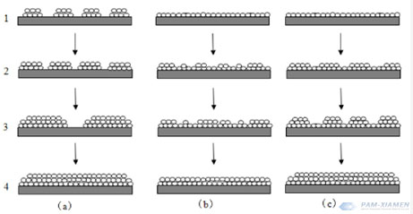
Island growth is easy to grow 3C-SiC on 4H-SiC. In order to prevent the defects of silicon carbide, the growth needs to be controlled as layered growth. However, the pure carbon-silicon bilayer will undergo mixed growth – even if it is layered growth at the beginning, it will begin to grow defects in silicon carbide single crystals in other types later.
The reason can be analyzed microscopically: if the deposited gas atoms are regarded as a hexahedron, the surface of a piece of substrate is divided into terrace, step, and kink, which is based on the number of contact surfaces. All the three are called TLK structure:
- The contact surface between the mesa and the deposited atom is 1;
- The contact surface between the step and the deposited atom is 2;
- The contact surface between kinks and deposited atoms is 3.
The contact surface of the step is more than that of the mesa, and the effect of deposited atoms and substrate atoms is stronger. In this way, the role of deposited atoms and substrate atoms> the role of deposited atoms and deposited atoms can be realized. Therefore, the single crystal is generally cut at a certain off-angle to obtain a substrate or seed crystal with off-angle, so that the mesa becomes a step.
Step-controlled epitaxy growth of silicon carbide: Use a substrate with an off-angle to the (0001) plane to build more steps, reducing the silicon carbide defects, such as mesa and prevent spontaneous nucleation, then further prevent the formation of 3C-SiC.

Fig. (a) Two-dimensional growth model of 3C-SiC
Fig. (b) 4H-SiC Homoepitaxial Step Flow Growth Model
3C-SiC nucleation will still occur on low-off-angle substrates with a deviation of 4° and below, resulting in triangular defects. Triangular defect = two basal plane dislocations + stacking faults, two basal plane dislocations extend into a hypotenuse, and the middle is a stacking fault, which is easy to directly collapse. To avoid silicon carbide defects, it needs to control temperature, air flow and other conditions.

For more information, please contact us email at victorchan@powerwaywafer.com and powerwaymaterial@gmail.com.