Silicon carbide has a variety of crystal types, but the silicon crystal structure the market needed is mainly 4H-SiC. So the silicon carbide crystal growth in crystal types is a defect. To a certain extent, it can be distinguished by the naked eye. A more accurate measurement method for testing the silicon carbide crystal distribution is Raman spectroscopy: Raman spectroscopy has characteristics for crystals, and the peak positions of the light emitted by different crystals are different.
1. What is Raman Spectroscopy?
In 1928, Indian scientist Raman discovered Raman scattering in the experiment of studying the scattering spectrum of liquid benzene. Raman scattering spectroscopy, in simple terms, is that use a beam of light incident on a substance, the frequency of the incident light is v, and the frequency of the resulting scattered light will be v, v+Δv1, v-Δv1, v+Δv2, v-Δv2, and so on. These Δv1, Δv2, etc. Δv are with characteristics. In other words, each substance has a certain difference (peak position, peak intensity), which is called Raman shift(the emitted light minus the incident light).
For example, the Raman spectrum of 4H-SiC is:
| Raman shift(cm-1) | E2 transverse acoustic wave | E2 transverse acoustic wave | A1 transverse acoustic wave | E2 transverse acoustic wave | A1 transverse acoustic wave | A1 longitudinal acoustic wave | LOPC | LOPC |
| 4H-SiC | 194.958 | 204.034 | 610.031 | 776.489 | 796.861 | 963.106 | 964.769 | 994.643 |
The table above shown here is the Raman shift. During the silicon carbide crystal distribution measurement, the computer will help to calculate it and process it as a Raman shift spectrum.
2. How to Test the Silicon Carbide Crystal Distrubution?
Typical test conditions are: using the 532nm laser of the Ar+ laser of the LabRAM HR Raman spectrometer, it is incident vertically, the excitation power is 200mW, and the mode of collecting scattered light is the backscatter mode. The incident light with different wavelengths has different penetration depths. Generally, the 266nm laser is 0.2um, the 325nm laser is 2um, and the 514nm laser is 30um, which means that ultraviolet light can only be used to measure thin samples.
Because the silicon carbide wafer has different positions, multiple measurements will be taken to obtain the silicon carbide crystal distribution:
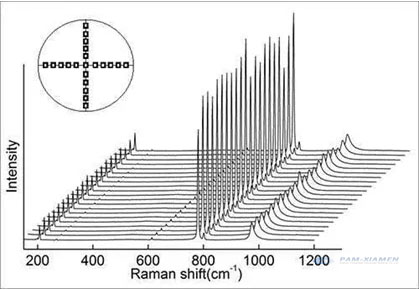
The data has three indicators: the position of the peak, the height of the peak (light intensity), and the width of the peak. Only when the peak position is completely matched, can it be the qualified 4H-SiC. As with XRD, whenever there are other peaks, they are substances of other phases, which is a defect.
The difference in the position of the peak is due to the difference in the energy of the phonons brought about by the different silicon carbide crystal lattices, that is, the different frequencies. Each phonon has its corresponding energy level. The virtual energy level theory can be used to explain Raman (non-linear process):
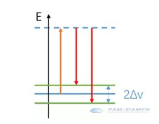
The particle absorbs incident light to the virtual energy level (orange), and then transitions back to a vibrational energy level(red) that is different from the original energy level. Because the upper energy level is a virtual energy level, the frequency of the incident light can be varied, as long as it does not conflict with the original real energy level.
It is worth noting that the LOPC mode (964.769 cm-1) can be used to analyze the carrier concentration:
n = 1.25 * 1017cm-2 *(964.769cm-1-VLOPC measurement)
As the carrier concentration increases, the interaction between atoms and the lattice increases, which makes the Raman peak blue shift (smaller), the intensity decreases, and the width increases. This method is not as accurate as other methods and can only be used as an aid to analyze the silicon carbide crystal distribution.
3. Why not Use XRD to Measure Silicon Carbide Crystal Distribution?
X-rays are optical radiation generated by the transition of electrons in the inner layer of atoms under the bombardment of high-speed moving electrons, including continuous X-rays and characteristic X-rays. Silicon carbide single crystal can be used as X-ray gratings, and the coherent scattering produced by these large numbers of particles (atoms, ions, or molecules) will cause light interference, increasing or decreasing the intensity of scattered X-rays. Due to the superposition of scattered waves from a large number of particles, the beams that interfere with each other to produce the highest intensity are called X-ray diffraction lines.
To meet the diffraction conditions, Bragg formula can be applied: 2dsinθ=nλ.
The incident beam causes each scatterer to re-radiate a small part of its intensity as a spherical wave. If the scatterers are arranged symmetrically with the interval d, these spherical waves will only be synchronized in the direction where their path length difference 2dsinθ is equal to an integer multiple of the wavelength λ. In this case, a part of the incident beam is deflected by an angle of 2θ, which will produce reflection points in the diffraction pattern.
Use X-rays of known wavelengths to measure the θ angle to calculate the interplanar spacing d, which is used for X-ray structure analysis; the other is to use a silicon carbide seed crystal with a known d to measure the θ angle to calculate the characteristic X-ray wavelength, and then the elements contained in the sample can be found in the existing data.
The measurement formula is 2dSinθ=λ. While the d value among the cubic silicon carbide crystal is close, and the characteristic is not obvious enough, the accurate silicon carbide crystal distribution cannot be precisely determined. For these reasons, it is not suitable to use the XRD to measure the distribution of silicon carbide crystals.

For more information, please contact us email at victorchan@powerwaywafer.com and powerwaymaterial@gmail.com.