Xiamen Powerway Advanced Material Co., Ltd (PAM-XIAMEN) offers InSb crystal wafer up to 2″ in diameter that are grown by a modified Czochralski method from highly purified, zone refined polycrystalline ingots. More about the indium antimonide crystal substrate specifications, please see the following part:

1. Indium Antimonide Wafer Specifications
No. 1 Indium Antimonide (InSb) Substrate PAMP16052-INSB
| Item | 2 inch InSb Single Crystal Wafer |
| Type | Te doped, n-type |
| Orientation | (100)A±0.5° |
| Thickness | 525±25 um |
| Concentration | 3 ~8 x 1014 cm-3 |
| Mobility | > 4 x 10⁵ |
| Surface | Both sides polished* |
| EPD | <20 cm2 |
| *In (A), Face polished chemical, final face Sb (B), Face polished linde a 0.3 microns, mirror finish | |
No. 2 InSb Wafer PAM160121-INSB
| Item | 2 Inch InSb Wafer |
| Orientation | 100 |
| Type | N type/ undoped |
| Carrier Concentration | <E15 |
| EPD | <50/cm2 |
| Flat | EJ standard |
| Surface | single side polished (A Face) |
| Epi-ready, Ra<0.5nm |
No. 3 Indium Antimonide Wafer PAM160127-INSB
| Item | 2” Indium Antimonide (InSb ) Wafer |
| Type | N-Type, Tellurium doped |
| Thickness | 525±25 um |
| Orientation | (100)A±0.5° |
| Carrier Concentration (77K) | 3 ~8 x 1014 cm-3 |
| Mobility | >4E5 cm2v-1s-1 |
| EPD | <100 cm-2 |
| Minority Carrier lifetime | > 8 x 10⁻⁷ sec |
| Euro-Japanese Major Flat: | 16 mm (+/- 1 mm) on the (0_11) +/- 0.5° |
| Euro-Japanese Minor Flat: | 8 mm (+/- 1 mm) on the (_211) +/- 0.5° |
| Surface | In (A) Face Polished Chemical, Final Face |
| Sb (B) Face Polished Linde A 0.3 microns (mirror finish) |
2. Indium Antimonide Properties
Indium antimonide is silvery, brittle, and has a zinc blende structure. The indium antimonide constant is 6.48 Å, which is a direct band gap material with a narrow band gap of 0.18 eV. The electron mobility is as high as 7800 cm2/V·s. The melting point of indium antimonide is 525°C. Compared with other III-V group compounds, it is more easy to purify and grow single crystals. More basic properties please see the figure below:
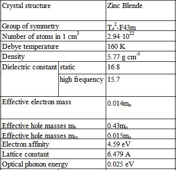
InSb Properties at 300K
Following diagram shows the indium antimonide carrier concentration and band structure at 300K:

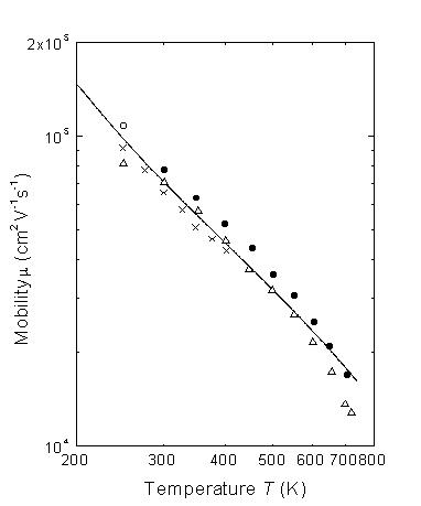
The InSb Electron Mobility is changes with the temperature:
3. Indium Antimonide Single Crystal Wafer Preparation
The InSb single crystal is prepared by the Czochralski method, and the raw material InSb is purified by zone melting. In InSb material, except for tellurium, the effective segregation coefficient is close to 1, and the effective segregation coefficient of other harmful impurities is less than or greater than 1. Meanwhile, the purity of indium antimonide substrates can be effectively improved.
The basic process of CZ growth is that the melt is kept in high-purity hydrogen or high-purity nitrogen containing high-purity H210%-20% at a constant temperature of about 800℃ for 0.5h, which can effectively remove scum on the surface of the melt. It grows significantly along the <111> direction, and the facet effect caused by the radial carrier distribution is very uneven. The growth is along with <100>, <115>, <113> and other crystal directions, and the facet effect can be eliminated. InSb, in addition to D pits, S pits (dish-shaped pits) and P pits (puching-out) are also observed. There are D pits, S pits (dish-shaped pits) and P pits (puching-out) in the indium antimonide thin films. The indium antimonide doped with isoelectronics (such as N doping) can reduce the density of these defects.
4. Challenge for InSb (111) Wafer Manufacturing
Due to the particularity of the indium antimonide material, the electrical parameters of the InSb wafer processed by the crystal grown in the <111> direction are poor, and cannot meet the needs of the focal plane device. Therefore, the InSb crystal must be grown in the <211> direction and then cut the crystal through the <111> direction to obtain the indium antimonide <111> wafer. Due to the anisotropic nature of the crystalline material, when growing a single crystal ingot in the <211> direction, the growth rate is different in each direction, so the growth interface is not approximately circular, but a “D” shape or trapezoid.
The difference in the growth interface eventually leads to different shapes of the two indium antimonide ingots grown in different directions. The equal-diameter part of the ingot grown in the <111> direction is similar to a cylinder. The equal-diameter part of the ingot grown in the <211> direction is similar to a dam. Such ingots grown in the <211> direction need to be rotated at a certain angle when cutting in the <111> direction. Since the rotation direction is perpendicular to the large surface, the height of the trapezoid can be increased to a certain extent, thereby reducing the height ratio of the bottom side. This increase in height still has a considerable difference in size from the large base, and the height is often only half the size of the base. This kind of irregularity is a huge challenge for the standardized process of indium antimonide wafers.
5. InSb Single Crystal Wafer Applications
Epi-ready single crystal InSb substrate with surafce roughness less than 0.5 nm is suitable for molecular beam epitaxy (MBE) growth. At the same time, because Indium antimonide conduction electron is high, InSb prime wafer is a good substrate material for infrared detectors, Hall devices, magnetoresistive devices, synchronization of IR and visible pulses in pump-probe setup and etc.
For example, imaging devices and indium antimonide focal plane array devices corresponding to the 3 to 5 μm band of the atmospheric transmission window. In addition, in charge injection devices, the number of InSb devices has reached 128×128 arrays. The hybrid focal plane array composed of 3~5μm waveband InSb photovoltaic detectors as sensitive elements has also been greatly developed, and it has been made into a two-dimensional array with a large number of elements.
Except for the InSb substrates, GaSb wafer in 2 inch also can be offered by PAM-XIAMMEN, take the below one for example:
2” Gallium Antimonide Substrate
Thickness:525±25µm,
Orientation:[111B]±0.5°,
Type/Dopant:P/undoped; N/undoped
Polish:SSP; DSP
Surface Condition and other Specification
6. FAQ of InSb Substrate
Q1: Could you please tell us when we open which surface of InSb wafer is A (In) and which surface is B (Sb)?
A: We just recognize it by two flats of the indium antimonide substrate, please contact victorchan@powerwaywafer.com for the drawing of the flats.
Q2: We would like to make use of the high nonlinear refractive index of InSb, fabricate an InSb waveguide, and excite the supercontinuum from it, pumped by a mid-infrared laser. So we need some InSb wafers for testing the waveguide etching parameters. I guess the dummy grade would be good enough, am I right?
A: Yes, you are right that it’s enough to use InSb substrate at dummy grade for testing the waveguide etching parameters.
Q3: What is the thickness of the surface oxide layer on epi-ready grade InSb substrate? Also, if there is no Sb flux, and thermal deoxidation cannot be performed directly, do you have any treatment methods for Ar ion or H atom? If treated with Ar or H, do we need to use acid to corrode the oxide layer first?
A: The thickness of the surface oxide layer on InSb is generally ** angstroms. ** treatment requires specialized equipment and is best to connected to the growth equipment (the chamber can be connected) for better results. ** should not be used before treatment (it is used immediately after opening the box and has a high surface cleanliness). Please contact victorchan@powerwaywafer.com to obtain the specific value of “**”.

For more information, please contact us email at victorchan@powerwaywafer.com and powerwaymaterial@gmail.com.