Dummy grade single crystal indium phosphide wafer is available with doping S grown by VGF. The electron concentration of the N-type indium phosphide wafer reaches 1018cm-3, and the indium phosphide resistivity is very low, generally 10-2~10-3Ω·cm. It is mostly used in high-speed optoelectronic devices, such as LD, LED, PIN- PD, PIN-APD and etc. EPD map of InP can be offered if necessary, please contact us at victorchan@powerwaywafer.com. The specifications of the test grade InP wafers are listed as follows:
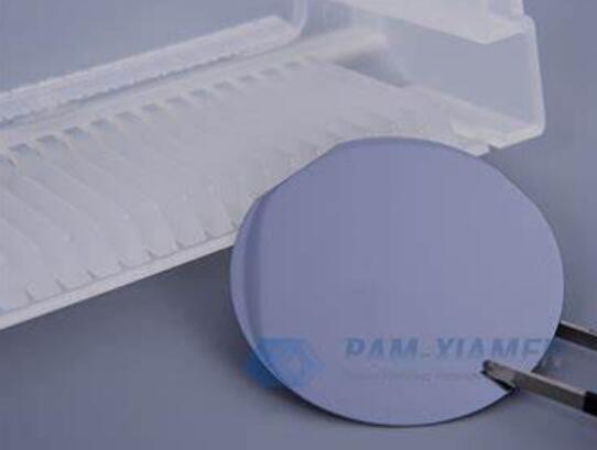
1. Specifications of Indium Phosphide Wafer at Dummy Grade
Item 1:
| Item | Parameter | UOM |
| Material | Indium Phosphide Wafer | |
| Grade | Dummy Grade | |
| Diameter | 50.0 ± 0.5 | mm |
| Thickness | Min: 300 Max: 400 | um |
| Orientation | (100) ± 0.5° | |
| Conductivity Type / Dopant | S-C-N / S | |
| Primary Flat Length | 16 ± 2 | mm |
| Primary Flat Orientation | EJ(0-1-1) | |
| Secondary Flat Length | 7 ± 1 | mm |
| Secondary Flat Orientation | EJ(0-11) | |
| Carrier Concentration | Min: / Max: / | cm-3 |
| Resistivity | Min: / Max: / | ohm-cm |
| Mobility | Min: / Max: / | cm2/V*Sec |
| EPD | Ave: / Max: <1000 cm-2 | cm-2 |
| TTV | 10 | um |
| TIR | 10 | um |
| BOW | 10 | um |
| Warp | 15 | um |
| Surface | P/P, P/E | |
| Edge Rounding | 0.25 (Conform to SEMI Standards) | mmR |
| Epi-ready | Yes | |
| Laser Mark | / | |
| Lamellar twin area | useful single crystal area with (100) orientation >80% | |
| Package | individual container filled with N2 |
Item 2:
| Item | Parameter | UOM |
| Material | Indium Phosphide Substrate | |
| Grade | Dummy Grade | |
| Diameter | 76.2 ± 0.5 | mm |
| Thickness | Min: 600 Max: 650 | um |
| Orientation | (100) ± 0.5° | |
| Conductivity Type / Dopant | S-C-N / S | |
| Primary Flat Length | 22 ± 1 | mm |
| Primary Flat Orientation | EJ | |
| Secondary Flat Length | 12 ± 1 | mm |
| Secondary Flat Orientation | EJ | |
| Carrier Concentration | Min: / Max: / | cm-3 |
| Resistivity | Min: / Max: / | ohm-cm |
| Mobility | Min: / Max: / | cm2/V*Sec |
| EPD | Ave: / Max: <1000 cm-2 | cm-2 |
| TTV | 10 | um |
| TIR | 10 | um |
| BOW | 10 | um |
| Warp | 15 | um |
| Surface | P/P, P/E | |
| Edge Rounding | 0.25 (Conform to SEMI Standards) | mmR |
| Epi-ready | Yes | |
| Laser Mark | / | |
| Lamellar twin area | useful single crystal area with (100) orientation>80% | |
| Package | individual container filled with N2 |
Item 3:
| Item | Parameter | UOM |
| Material | Indium Phosphide Wafer | |
| Grade | Dummy Grade | |
| Diameter | 100.0 ± 0.5 | mm |
| Thickness | Min: 600 Max: 650 | um |
| Orientation | (100) ± 0.5° | |
| Conductivity Type / Dopant | S-C-N / S | |
| Primary Flat Length | 32.5 ± 1 | mm |
| Primary Flat Orientation | EJ | |
| Secondary Flat Length | 18 ± 1 | mm |
| Secondary Flat Orientation | EJ | |
| Carrier Concentration | Min: / Max: / | cm-3 |
| Resistivity | Min: / Max: / | ohm-cm |
| Mobility | Min: / Max: / | cm2/V*Sec |
| EPD | Ave: / Max: <1000 cm-2 | cm-2 |
| TTV | 10 | um |
| TIR | 10 | um |
| BOW | 10 | um |
| Warp | 15 | um |
| Surface | P/P, P/E | |
| Edge Rounding | 0.25 (Conform to SEMI Standards) | mmR |
| Epi-ready | Yes | |
| Laser Mark | / | |
| Lamellar twin area | useful single crystal area with (100) orientation>80% | |
| Package | individual container filled with N2 |
2. Dummy Grade Indium Phosphide Applications
Dummy grade InP wafer is used for epi growth process test and composition characterization on the epitaxial layer. It is not suitable for etching device structures, e.g. waveguide and optical grate because of twin crystals and possible holes of the wafer orientation on the twin side.
Microtwin or lineage of the wafer surface < 20% is acceptable.
3. Indium Phosphide Properties
Indium phosphide is a group III-V compound semiconductor material compounded by the combination of group III element indium (In) and group V element phosphorus (P). It has a zinc blende structure with a indium phosphide lattice constant of 0.586 9 nm. InP single crystal is soft and brittle, silver-gray with metallic luster. The indium phosphide band gap at room temperature is 1.344 eV, which is a direct transition band structure. The emission wavelength is 0.92 um, the intrinsic carrier concentration of InP at room temperature is 2×107 cm-3, and the electron and hole mobility are 4 500 cm2/V-s and 150 cm2/V·s respectively.

Indium Phosphide Crystal Structure
4. InP Wafer Manufacturing Process
Indium phosphide has almost the same face-centered cubic crystal structure as gallium arsenide GaAs and most III-V semiconductors. Indium phosphide wafers must be prepared before device manufacturing and must be overlapped to eliminate surface damage during slicing. The dummy wafer of InP is then chemical mechanical polishing (CMP) for the final material removal stage, allowing to obtain a mirrored surface with atomic-scale ultra-flat roughness.
However, the growth process of indium phosphide from raw materials to ingots to wafers is very difficult. During the growth process, a high temperature of 1070℃ and extreme pressure are required. In addition, the atomic structure may change. What comes out may not meet expectations. From raw materials to ingots to a 2-inch or 4-inch indium phosphide single crystal wafer, the yield is generally about 28%, and the technical threshold is very high. Therefore, PAM-XIAMEN is one of the indium phosphide wafer suppliers that can successfully control the growth technology of indium phosphide. Relying on VGF, VB method crystal growth technology, high surface quality wire cutting technology, ultra-flat mechanical chemical polishing technology, ultra-clean surface cleaning technology and other related core technologies, the commercialization of indium phosphide wafers tends to be stable, and the products provided by PAM-XIAMEN are mainly used in optical fiber communications, optical detectors, infrared optics, high-frequency millimeter wave communications and other fields. In addition to the current application areas, the monocrystalline indium phosphide wafer substrate will expand in the terahertz field used in 6G communications.
5. InP Material Future Development
In fact, InP substrate material is the most critical core material in the optical communication industry chain, ultra-high frequency millimeter wave radar, infrared detection and other fields. It is inseparable from indium phosphide since the demand for higher bandwidth continues to grow, especially in the Human-driven cars, 5G communications, even the implementation and application of 6G, 7G, and 8G in the future. The indium phosphide wafer market at dummy or prime grade will usher in rapid growth, thereby, the indium phosphide wafer cost will go down.

For more information, please contact us email at victorchan@powerwaywafer.com and powerwaymaterial@gmail.com.