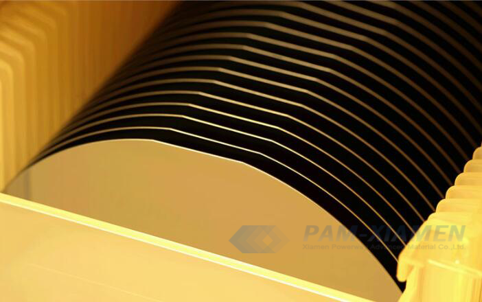
Xiamen Powerway Advanced Material Co.,Ltd., a leading supplier of InGaAs (Indium Gallium Arsenide) wafer and other related products and services announced the new availability of size 2″ is on mass production in 2017. This new product represents a natural addition to PAM-XIAMEN’s product line.
Dr. Shaka, said, “We are pleased to offer GaInAs wafer to our customers including many who are developing better and more reliable for infrared detector and HEMT devices using InGaAs channels. Our InGaAs wafer has excellent properties, single crystal epitaxial films of indium gallium arsenide can be deposited on a single crystal substrate of III-V semiconductor having a lattice parameter close to that of the specific gallium indium arsenide alloy to be synthesized. Three substrates can be used: GaAs, InAs and InP. The availability improves boule growth and wafering processes.” and “Our customers can now benefit from the increased device yield expected when developing advanced transistors on a square substrate. Our GaInAs wafer are natural by products of our ongoing efforts, currently we are devoted to continuously develop more reliable products.”
PAM-XIAMEN’s improved GaInAs product line has benefited from strong technology, which is supported from Native University and Laboratory Center.
1. Specifications of InGaAs/InP Epi Wafer
No.1 InGaAs Photodetector Wafer on InP Substrate
PAM200624-INGAAS LAYER ON INP
| Material | Doping (cm-3) | Thickness (nm) |
| P++ InGaAs | 1.4*1019 (C) | – |
| P+ InGaAs | – | 100 |
| i-InGaAs | No dopping | – |
| n+ InP | – | 400 |
| i-InGaAs | No dipping | – |
| i-InP | – | 50 |
| Semi Insulator InP | Fe | Substrate |
Note: In the structure, InGaAs is generally doped with Zn. If C is doped, the concentration may be lower, and the quality of materials with high concentration of C will be worse. So Zn doped is suggested.
No.2 Epitaxial GaInAs on InP
PAMP19330-GAINAS
| Layer | Material | Concentration (cm3) | Thickness(nm) |
| p-contact | p++- InGaAs, p+ InP | 1.0 x10¹⁹ (Zn), 1.0 x10¹⁸(Zn) | 100, 100 |
| i-layer/absorber | i-InGaAs | n.i.d | – |
| n-contact | n+ InP | – | – |
| Etch-stop | i-InGaAs | n.i.d | 50 |
| buffer | i-InP | n.i.d | – |
| substrate | S.I InP | Fe |
2. About GaInAs Material
Indium gallium arsenide (alternatively gallium indium arsenide) is a ternary alloy (chemical compound) of indium, gallium and arsenic. Indium and gallium are both from boron group (group III) of elements while arsenic is a pnictogen (group V) element. Thus alloys made of these chemical groups are referred to as “III-V” compounds. Because they are from the same group, indium and gallium have similar roles in chemical bonding.
InGaAs semiconductor, which is a room-temperature semiconductor applicable for electronics and optoelectronics, has characteristics between GaAs and InAs. Since electrons travel several times faster in GaInAs than in silicon, the InGaAs technology is ideal for fabricating a high speed, high sensitivity photodetector, which is the first choice for fiber optic communications. By far, the most important alloy composition from a technical and commercial point of view is Ga0.47In0.53As, which can be deposited on indium phosphide in a single crystal form.
3. Properties of Indium Gallium Arsenide Epilayer
When GaInAs thin film can epitaxial on an III-V compound substrate, a good match between the lattice constants of the film and the substrate is necessary to maintain the single crystal properties, a limitation that allows small changes in composition on the order of a few percent. Therein, InGaAs InP lattice matched at 295K when the In composition is 0.53. At the moment, the InGaAs bandgap is 0.75eV, the electron effective mass is 0.041, and the electron mobility of GaInAs is close to 10,000 cm2•V−1•s−1 at the room temperature.
4. FAQ about Indium Gallium Arsenide Epi on InP Substrate
Q: Could we have a quotation of InGaAs epi wafer on InP substrates?
Absorption wavelength Range: 1540nm-1570nm
thickness:>500nm
A: Yes, we can grow single epi of 1um InGaAs thin film on InP substrate, but the absorption wavelength range is 950-1650nm. Based on our experience for epitaxy, only by adding the REC reflector, can the absorption wavelength range be as close as possible to the wavelength of 1540nm-1570nm.

For more information, please contact us email at victorchan@powerwaywafer.com and powerwaymaterial@gmail.com.