A gradient is a material that has a specific molecule on its surface, with the concentration of the molecule sloping from a high concentration on one end to a low concentration at the other end. The gradient is used not only to determine whether other molecules interact with the molecules on the gradient, but to determine the threshold level at which any interactions take place.
Now, researchers from North Carolina State University (NC State) have developed a new technique for creating biomolecular gradients that is both simpler than existing techniques and that creates additional surface characteristics that allow scientists to monitor other aspects of molecular behaviour.
And the gradient material they have used to investigate this is indium gallium nitride (InGaN).
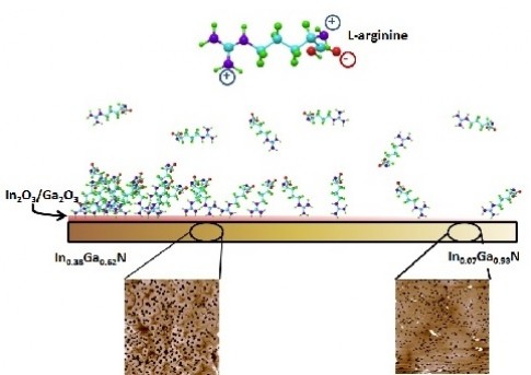
The new technique begins with a substrate made of InGaN. Negatively-charged oxides form on the surface, which then bind to the amino acid L-arginine. (Image credit: Lauren Bain)
The new technique begins by creating an InGaN substrate. The substrate itself is a gradient, sloping from an indium-rich end to a gallium-rich end. The indium-rich end is more conducive to the formation of oxides. When exposed to humidity, negatively charged indium and gallium oxides form on the surface of the substrate.
The researchers then put the substrate into a solution that contains an amino acid called L-arginine, which is positively charged at biologically relevant pH levels, such as those found in the human body.
“The L-arginine binds to the negatively charged oxides on the surface of the substrate,” says Lauren Bain, a Ph.D. student at NC State who is lead author of a paper on the work. “Because there is more oxide accumulation at the indium-rich end, there is a higher concentration of L-arginine at that end, and the concentration gradually declines along the surface of the substrate as you move toward the gallium-rich end.”
“We studied L-arginine because it is small, but relevant. Because it is small, we could easily assess what was happening during our study,” Bain says. “But because it is a building block for proteins, we can build on this work to study full peptides and proteins, such as ligands that bind to cell receptors.”
“This technique also creates changes in the topography of the InGaN’s surface, based on the different crystalline structures within the material as its shifts from being indium-rich to being gallium-rich,” explains Albena Ivanisevic, an associate professor at NC State and senior author of the paper. “This allows us to assess topographical differences in molecular adhesion, which is important, given the variety of topographies found in biological systems.”
A paper describing this work “Biomolecular Gradients via Semiconductor Gradients: Characterization of Amino Acid ,Adsorption to InxGa1-xN Surfaces.” by Lauren E. Bain et al was published online in July 2013, ACS Applied Materials and Interfaces. DOI: 10.1021/am4015555
The substrate development for this project was proposed by Tania Paskova, a professor of electrical and computer engineering at NC State. The actual substrate was prepared in the lab of NC State professor Salah Bedair.
Source:CS
If you need more information about Graded InGaN Enlightens Us On Molecular Interactions, please visit our website:https://www.powerwaywafer.com/, send us email at sales@powerwaywafer.com or powerwaymaterial@gmail.com