PAM-XIAMEN can offer InGaSb material substrate, which can be used for InGaSb photodetectors, InGaSb/GaAs quantum dots (QDs), InGaSb-on-insulator for p-MOSFET, and InGaSb/InAs superlattice materials for infrared photodiodes in the very long-wavelength infrared (VLWIR) range
It can be grown on GaAs substrate, GaSb (111)A substrate and GaSb(111)B substrate by MBE, and now please see below spec:
2”, 1um,InGaSb epi layer on GaAs substrate.
Diameter – 50.8±0.5 mm;
Orientation – (100)±0.5°
Substrate thickness – 350±25 µm;
Epi layer:1um
Flat– SEMI-E/J;
Front side- polished, epi-ready;
Back side – etched
Package – each are packed in single wafer container, in the package of aluminium foil bag filled with an inert gas.
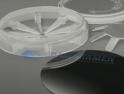
InGaSb Film on GaAs Substrate
For more information, please contact us email at victorchan@powerwaywafer.com and powerwaymaterial@gmail.com