PAM-XIAMEN can provide InP laser structure with InAlGaAs quantum well for 1300nm lasers. InGaAsP / InP and AlGaInAs / InP quantum well material systems have become the most widely used gain media. Compare with InGaAsP / InP material, AlGalnAs / InP has larger conduction band offset than InGaAsP / InP material, so it can more effectively prevent the leakage of streamers under high temperature and high injection, and improve the high-temperature characteristics of the laser device. The AlGaInAs / InP material system is at 1.3um and 1.55um laser structures have been widely used. Take the epitaxial structure based on AlGaInAs / InP quantum well for example:
1. Epi-structure of InAlGaAs / InP Laser Diode
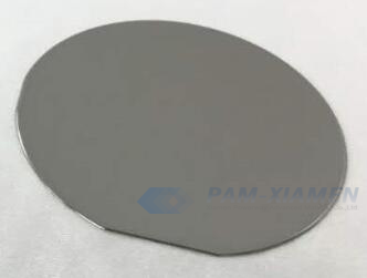
No.1 3inch InP Epitaxy Structure PAMP22246 – 1300LD
| Layer No. | Epi Layer | Material | Doping(cm-3) | Thickness(um) | Al | Ga | In | P | As |
| 15 | Cap | InP | undoped | – | |||||
| 14 | Cap | InGaAs (lattice matched) | – | – | 0.15 | 0.85 | – | – | |
| 13 | Super Lattice | n-type InP | – | – | |||||
| 12 | Super Lattice | n-type InGaAsP | – | – | – | – | – | ||
| 11 | N-contact | n-type InP | – | 0.13 | |||||
| 10 | Barrier | InAlGaAs | – | – | – | – | – | – | |
| 9 | Quantum Well | InAlGaAs | – | – | – | – | – | – | |
| 8 | Barrier | InAlGaAs | – | – | – | – | – | – | |
| 7 | Electron Blocking | InAlGaAs | – | – | – | – | – | – | |
| 6 | SCH | p-type InAlGaAs | 1.00E+17 | – | – | – | – | – | |
| 5 | Cladding | p-type InP | – | 1.5 | |||||
| 4 | P-contact Layer (lattice matched) | P-type InGaAs | – | – | – | – | – | ||
| 3 | Etch Stop | InP | – | – | |||||
| 2 | Etch Stop | InGaAs | undoped | – | – | – | – | ||
| 1 | Buffer | InP | – | – | |||||
| Substrate | InP |
No. 2 3inch III-V Epitaxy PAMP21120 – 1300LD
| Layer No. | Layer Type | Material | PL wavelength (nm) | Thickness(nm) | Dopant | Type |
| 11 | sacrificial | InP | – | – | – | |
| 10 | sacrificial | GaInAs | – | – | – | |
| 9 | bonding layer | InP | – | – | – | |
| 8 | InP | – | Si | N | ||
| 7 | AlGaInAs MQW | 1280~1310 | – | – | – | |
| 6 | InP | – | Zn | P | ||
| 5 | GaInAsP | – | – | – | ||
| 4 | GaInAs | 170 | – | – | ||
| 3 | InP | – | – | – | ||
| 2 | etch stop | GaInAs | – | – | – | |
| 1 | buffer | InP | – | – | – | |
| 0 | substrate | InP |
2. Why Grow InAlGaAs Material as Quantum Well for InP Laser Fabrication?
AlGalnAs is a rapidly developing alternative material in recent years. InAlGaAs is an ideal material for high-temperature uncooled semiconductor lasers due to the following characteristics:
1) AlGaInAs only has one V-group element, making it easier to control the growth quality of the material, which is conducive to achieving good luminescent zone performance.
2) Compared to InGaAsP material, the refractive index of AlGalnAs material with the same bandgap is higher than that of InGaAsP material, making indium phosphide laser devices not only have large electron confinement but also greater optical confinement;
3) Due to the tensile strain effect of AlGaInAs quantum wells compared to InP substrates, tensile strain can provide better band separation and gain levels;
4) The conduction band bias of InAlGaAs / InP is large, and it has a strong ability to prevent electrons from overflowing the quantum well at high temperatures. The high-temperature characteristics of AlGaInAs / InP MQW lasers are much better than those of InGaAsP / InP MQW lasers. At the same time, the strain effect improves the valence band structure of quantum wells, reduces Auger recombination and valence band absorption, increases transparent carrier concentration and quantum efficiency, and further improves epi laser device temperature characteristics.
Remark:
The Chinese government has announced new limits on the exportation of Gallium materials (such as GaAs, GaN, Ga2O3, GaP, InGaAs, and GaSb) and Germanium materials used to make semiconductor chips. Starting from August 1, 2023, exporting these materials is only allowed if we obtains a license from the Chinese Ministry of Commerce. Hope for your understanding and cooperation!

For more information, please contact us email at victorchan@powerwaywafer.com and powerwaymaterial@gmail.com.