PAM XIAMEN offers InP Wafer. Detailed wafer information, please refer to below:
1. InP Wafer Specifications
InP(100)
InP (100) Sn-doped
InP-(VGF- Grown) (100) Sn doped, 2″x0.35mm wafer, 1sp
InP (100)undoped
InP (100) undoped, 10×10 x 0.5 mm wafer, 1sp
VGF InP (100) undoped, 2″ x 0.35 mm wafer, 1sp
VGF InP (100) undoped, 2″ x 0.35 mm wafer, 2sp
InP(100) Zn-doped
InP ,Growing Method: VGF(100) Zn doped,3 ” x 0.625mm, wafer, 1sp
VGF InP (100) Zn doped, 2″ x 0.35mm, wafer, 1sp
InP(100) Fe -doped
VGF InP (100) Fe doped, 2″x0.35 mm wafer, 1sp
InP(100) s-doped
InP-(VGF- Grown) (100) S doped, 2″x0.5mm wafer, 1sp
InP-VGF- (100) S doped, 10x10x0.5mm wafer, 2sp
InP(110)
InP-VGF Grown (110) undoped, N-type, 2″x0.5 mm wafer, 2sp
VGF InP (110) Fe doped, 2″x0.5 mm wafer, 2sp
InP(111)
InP-(VGF- Grown) (111)A S doped, 2″x0.5mm wafer, 1sp
InP-(VGF- Grown) (111)A Zn- doped, P-type ,2″x (0.3-0.35) mm wafer, 1sp
InP-(VGF- Grown) (111)B S doped, 2″x0.35mm wafer, 1sp
InP-VGF Grown (110) undoped, N-type, 2″x0.5 mm wafer, 2sp
InP-VGF Grown (111)A undoped, 2″x0.35 mm wafer, 1sp
InP-VGF Grown (111)A undoped, 5x5x0.5 mm wafer, 1sp
InP-VGF Grown (111)A Fe doped, 2″x0.35 mm wafer, 1sp, Semi-insulating
InP-VGF Grown (111)A Fe doped, 2″x0.35 mm wafer, 2sp, Semi-insulating
InP-VGF Grown (111)B undoped, 2″x0.35 mm wafer, 1sp
InP-VGF Grown (111)B Fe doped, 2″x0.35 mm wafer, 1sp, Semi-insulating
2. FAQ for InP Wafers
Q1: As I am aware off, on III/V wafers, always one side is considered as In and the other side P side of the InP wafer.
At least our last purchase of InSb wafers was lie this. We have to define for customer, which side is the In side and which side the Sb side. Or call IT Side A and Side B.
If the spider side is the backside, eventual this is the B-Side, but we still don’t know, for InP substrate, which side typically it will be In or P?
A: Not all wafers has In side or P side(take InP wafer as an example), only when it is (111)orientation, the wafer has In side and P side. That is why it is called (111)A or (111)B.
Q2: I was also wondering how I could cut InP wafers. I would like to have them diced using a machine, but was wondering:
1) if they can be exposed to water.
2) if it be possible to cut the wafers using diamond scribes.
A: You can use a blade to cut InP wafers along the cleavage surface (parallel flats). Cutting in air is no problem. Of course, you can cut in water. The blade should be thin, and you can use ordinary blade, because Indium phosphide is very soft, so the cut surface is plane (i.e. cleavage surface).
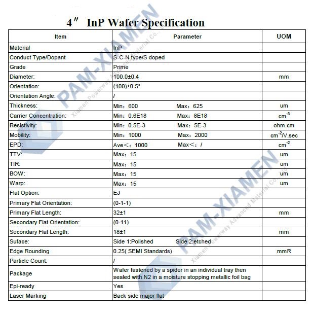
Q3: The application of InP wafers will be in manufacturing of InGaAs sensors with integrated ASIC electronic circuitry for 1.7 –2.6 µm. Could you please recommend us some suitable specifications ?
A: In terms of InP substrate for InGaAs sensor application, we will recommend the spec as figure shown below:
For more information, please contact us email at victorchan@powerwaywafer.com and powerwaymaterial@gmail.com.
Found in 1990, Xiamen Powerway Advanced Material Co., Ltd (PAM-XIAMEN) is a leading manufacturer of semiconductor material in China. PAM-XIAMEN develops advanced crystal growth and epitaxy technologies, manufacturing processes, engineered substrates and semiconductor devices. PAM-XIAMEN’s technologies enable higher performance and lower cost manufacturing of semiconductor wafer.
PAM-XIAMEN develops advanced crystal growth and epitaxy technologies, range from the first generation Germanium wafer, second generation Gallium Arsenide with substrate growth and epitaxy on III-V silicon doped n-type semiconductor materials based on Ga, Al, In, As and P grown by MBE or MOCVD, to the third generation: Silicon carbide and Gallium Nitride for LED and power device application.