Xiamen Powerway offers InSb (indium antimonide) epi wafer with homogeneous structure, which can be used to detect infrared radiation with a wavelength of 8~12um. Homoepitaxial InSb epi wafer on InSb substrate can improve the operating temperature of indium antimonide detector.
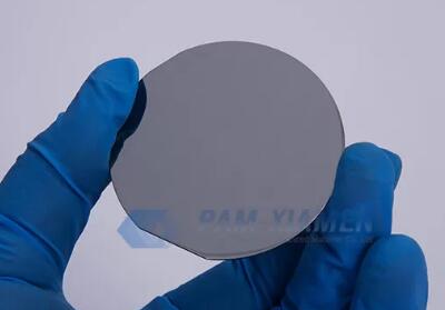
InSb epi ready wafer
1. InSb Homogeneous Structures
1.1 InSb Epi Wafer Structure (PAMP19142-INSBE)
|
InSb Epitaxial Wafer |
||||
| Epi Layer | Layer Composition | Thickness | Dopant | Doping Concentration |
| 4th Layer | InSb | 1000nm | Be (p+) | – |
| 3rd Layer | In(1-x)Al(x)Sb (x=0.15) | – | Be (p+) | 2.0E18cm-3 |
| 2nd Layer | InSb | 250nm | Si (n-) | – |
| 1st Layer | InSb | – | Si (n+) | 3.0E18cm-3 |
| Substrate | Te doped InSb | |||
| Thickness | 500 um | |||
| Doping Concentration | E17~E18 | |||
1.2 InSb Epitaxial Structure
|
InSb Epi Wafer |
||||
| Epi Layer | Layer Composition | Thickness | Dopant | Doping Concentration |
| 3rd Layer | InSb | 1000nm | Be (p+) | – |
| 2nd Layer | InSb | – | Si (n-) | 2.0E15cm-3 |
| 1st Layer | InSb | 4000nm | Si (n+) | – |
| Substrate | Te doped InSb | |||
| Thickness | 500 um | |||
| Doping Concentration | E17~E18 | |||
1.3 InSb Wafer <111> with InSb Epilayer on, By MOCVD or MBE Deposition
PAM200221-INSBE
| Item | Parameters | |
| Epi Layer | P-type InSb Layer, Be-Doped | <111> on the Sb face of substrate |
| Concentration | – | |
| Thickness of Epi Layer | – | |
| Minority Carrier Lifetime | >2E-10 sec. @77K | |
| Hole Mobility | >2.0E+3 cm2 / (V.sec) | |
| Substrate | N-type InSb | <111> ± 0.5 degree |
| Thickness | 500 ± 25 um | |
| Carrier Concentration | 3E+14~2E+15 cm-3, Te Doped | |
| EPD | <20cm-2 | |
| Electron Mobility | ≥1.0E+5 cm2 / (V.sec) | |
| Minority Carrier Lifetime | >8E-7 sec. @77K |
1.4 InSb Epitaxy Wafer
PAM200925-INSBE
| Epi Layer 3 | P-type epi layer: <111> on the Sb face of substrate |
| Concentration for epi layer: 5E+17cm-3, Be-doped | |
| Thickness for epi layer: 1um | |
| Minority carrier lifetime: >2E+10 sec. | |
| Hole mobility:>2.0E+3cm2/(V.sec) | |
| Epi Layer 2 | P-type epi layer: <111> on the Sb face of substrate |
| Concentration for epi layer: 1E+17cm-3, Be-doped | |
| Thickness for epi layer: 1um | |
| Minority carrier life time: >2E+10 sec. | |
| Hole mobility:>2.0E+3cm2/(V.sec) | |
| Epi Layer 1 | InSb: N type, Te-doped, <111>±0.5 |
| Thickness: 10um | |
| n=3E14~2E15cm-3 | |
| Electron mobility≥1.0E+5cm2/(V.sec) | |
| Minority carrier lifetime: >8E-7 sec.@77K | |
| substrate | N-type InSb, <111>±0.5 degree |
| Thickness: 500±25um | |
| Carrier concentration: 5E+15, Te-doped | |
| EPD<50cm-2 | |
| Electron mobility≥1.0E+5cm2/(V.sec) | |
| Minority carrier lifetime: >8E-7 sec.@77K |
2. Indium Antimonide Properties
Indium antimonide is a compound material with a direct bandgap, consisting indium and antimony elements. The indium antimonide energy band is 0.17 eV, which is small, but its electron mobility is very high. The indium antimonide constant is 0.648nm.
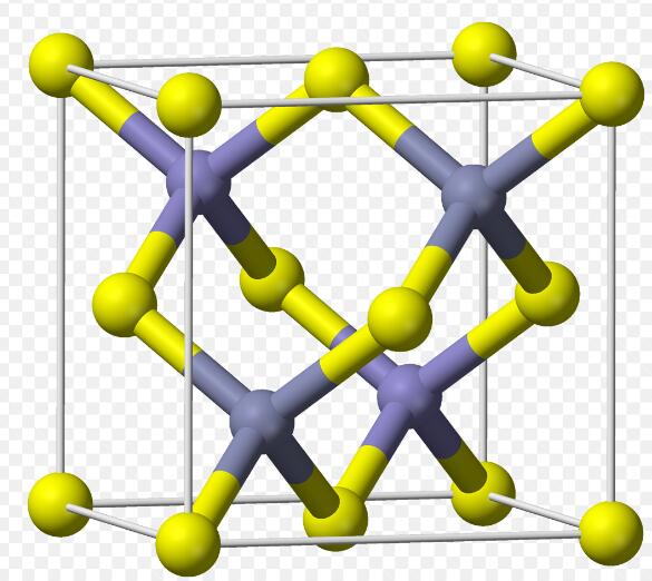
InSb Crystal Structure
3. Research on InSb Epi Wafer Technology
The surface state of the InSb substrate has a great influence on the crystal quality of the InSb thin film by the molecular beam epitaxy (MBE), and the surface oxide layer must be removed before epitaxy. The effective method for removing surface oxides is to perform wet chemical treatment on the InSb substrate before releasing into the MBE system to form a thinner oxide layer with a lower analytical temperature on the substrate surface. The following table lists the surface conditions of the substrate after treatment with different corrosives:
| Surface topography | Oxide layer thickness | Deoxidation temperature | |
| Mechanochemical polishing | Mirror | 6.5nm | >500℃ |
| Br-methanol | Smooth mirror | 6.3nm | >500℃ |
| CP4 | Orange peel | 3.1nm | – |
| Improved CP4 | Smooth mirror | 3.2nm | <500℃ |
The most important factors affecting the InSb MBE process are the growth temperature and the V/II beam current ratio.
3.1 Improve Growth Temperature for InSb Epi Growth Wafer
Growth temperature is one of the most important factors affecting the crystal quality of molecular beam epitaxial materials. Temperature affects the adhesion coefficient, growth rate, background impurity density, doping condition, surface morphology and the interface between different epitaxial layers. When the substrate temperature is too high, it is easy to cause the chemical ratio of the epitaxial film to deviate, causing In to precipitate and form defects. Meanwhile, it will affect the electrical properties of the epitaxial film. When the growth temperature is too low, the surface layer morphology becomes worse. The surface of the epitaxial thin film n/p doped InSb deposited onto semiconductor substrate is prone to form Hill-ock defects. Therefore, optimizing the growth temperature is one of the key steps in the development of the epi process and important means to reduce the InSb epi wafer defect. By using an InSb(100) substrate with an off-angle to reduce the growth temperature, after many experiments by PAM-XIAMEN epi wafer foundry, the optimized temperature is 400~450℃.
3.2 Optimize the beam ratio of V/II elements During the Indium Antimonide Epi Wafer Manufacturing Process
The beam ratio of V/II elements is very critical, and different beam ratios have a great influence on the surface morphology. Because the adhesion coefficient and migration speed of Sb and In atoms on the surface of the substrate are different, it affects the atomic arrangement on the surface of InSb, thereby affecting the reconfiguration of surface atoms, and ultimately affecting the nucleation of epitaxial films. Therefore, to obtain a high-quality InSb epitaxial film, an optimized range must be selected. RHEED is used to monitor the surface atomic reconstruction of InSb epitaxial film under different beam current ratios, and the quality of epitaxial film after epi process is used to find the optimal beam ratio range. After many experiments, PAM-XIAMEN found the optimized beam ratio is about 2~3 times.
All in all, to obtain high-quality InSb epi wafers, these parameters must be optimized.
4. FAQ for InSb Epi Wafer
Q1: Regarding the growth of InSb hetero-structures, what will be the growth technique MBE or MOCVD?
A: MBE technique will be used to grow InSb epi wafers.
Q2: What type of characterizations, you will provide along with InSb epitaxial wafers? We need at least thickness, doping and composition verification. If possible, we also need its absorption and photoluminescence spectroscopy measurements.
A: We will offer XRD measurement for InSb epitaxy.
Q3: Regarding characterization of the InSb wafer, it fine that you are providing XRD and PL measurements. Will it be possible to provide Hall Effect Measurement and FTIR?
A: Yes, we can offer FTIR measurement. We have FTIR equipment, absorption spectrum or transmission spectrum can be done for InSb epi.

For more information, please contact us email at victorchan@powerwaywafer.com and powerwaymaterial@gmail.com.