PAM-XIAMEN can provide etching silicon wafer in P type and N type, more specifications please see: https://www.powerwaywafer.com/silicon-wafer/etching-wafer.html. The etching of silicon wafers is divided into isotropy and anisotropy, shown as Fig. 1. Isotropy etching means that the etching rate of silicon in all directions is the same during the etching process, and the etching result is usually a groove-shaped structure; Anisotropy is opposite, which means that only the vertical direction of silicon is etched during the etching process, and the lateral direction is not etched. Through-silicon vias suitable for 3-D packaging can be fabricated by anisotropic etching.
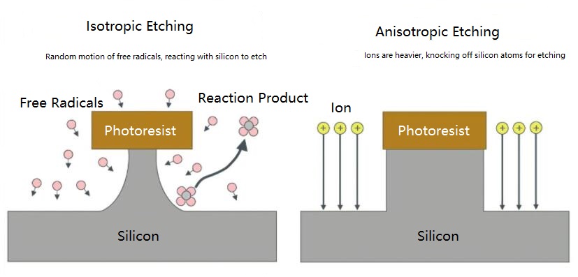
Fig. 1 Etching Schematic of Isotropic and Anisotropic
Silicon can be etched mainly by halogen-containing gases, such as Cl2. Although it can ensure a high degree of anisotropy in etching, its etching rate is low. We can use Br-containing gases, such as Br2 and HBr, but it has a lower etching rate. If it is too low, residues will be deposited on the silicon surface after etching. Therefore, most researchers use fluorine-based (F) chemical gases to etch silicon, but fluorine atoms react spontaneously with silicon materials, resulting in isotropic etching.
1. What is the Difference between Isotropic and Anisotropic Etching Different?
Silicon wafers have a single-crystal lattice structure that repeats in all directions, but with different densities in each direction. The vertical planes contain a different number of silicon atoms than the diagonal planes. This means that etching with certain etchants is slower in directions with more atoms and faster in directions with fewer atoms.
Etchants used for isotropic etching, such as hydrofluoric acid, etch at the same rate in all directions, independent of silicon atomic density. For etchants used for anisotropic etching, such as potassium hydroxide (KOH), the etch rate depends on the number of silicon atoms in the lattice plane, so the difference in the directionally anisotropic etch rate depending on the plane allows better control Shapes etched into silicon wafers. With the corresponding orientation of the silicon wafer, the etching can be timed to produce straight or angled sides and sharp corners. Etching under the mask can be reduced.
2. How to Use Isotropic and Anisotropic Etching in Semiconductor Manufacturing?
Isotropic etching is more difficult to control than anisotropic etching, but it is faster. During the initial stages of silicon wafer fabrication, large features are etched into the silicon. At this stage of fabrication, etch rate is important to facility throughput. Isotropic etching is used to quickly create these large shapes with rounded corners. Although process engineers and operators have less control over the shape of the features being etched, accurate temperature and concentration control is still important to ensure that the same circular shape is produced on wafers processed in different batches.
After etching large shapes with an isotropic process, the microstructures and metal paths require better control over the details. Anisotropic etching provides this control as long as the lattice structure of the silicon wafer is properly oriented. Anisotropic KOH etching is reliable and easy to control. It can be used to create precise, straight-edged shapes required for final semiconductor products. Precise control of temperature and etchant concentration is even more important for anisotropic etching. These process parameters strongly affect the etch rate in all directions, thus affecting the final shape of the etching.

For more information, please contact us email at victorchan@powerwaywafer.com and powerwaymaterial@gmail.com.