
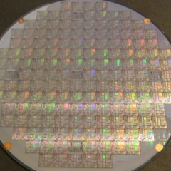
GaAs Epiwafer
PAM-XIAMEN is manufacturing various types of epi wafer III-V silicon doped n-type semiconductor materials based on Ga, Al, In, As and P grown by MBE or MOCVD. We supply custom GaAs epiwafer structures to meet customer specifications, please contact us for more information.
- Descrizione
Descrizione del prodotto
GaAs Epi wafer
As a leading GaAs epi wafer foundry, PAM-XIAMEN are manufacturing various types of epiwafer III-V silicon doped n-type semiconductor materials based on Ga, Al, In, As and P grown by MBE or MOCVD, which make a low gallium arsenide epi wafer defect. We supply custom GaAs epiwafer structures to meet customer specifications, please contact us for more information.
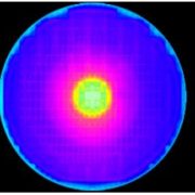
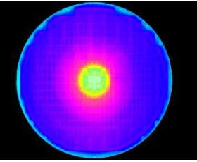
We have numbers of the United States Veeco’s GEN2000, GEN200 large-scale production of epitaxial equipment production line, full set of XRD; PL-Mapping; Surfacescan, and other world-class analysis and testing equipment. The company has more than 12,000 square meters of supporting plant, including world class super-clean semiconductor and a related research and development of the younger generation of clean laboratory facilities.
Specification for all new and featured products of MBE III-V compound semiconductor epitaxial wafer:
| substrato di materiale | Capacità materiale | Applicazione |
| GaAs | GaAs bassa temperatura | THz |
| GaAs | GaAs / GaAlAs / GaAs / GaAs | Diodo Schottky |
| InP | InGaAs | Rilevatore di PIN |
| InP | InP / InP / InGaAsP / InP / InGaAs | Laser |
| GaAs | GaAs / AlAs / GaAs | |
| InP | InP / InAsP / InGaAs / InAsP | |
| GaAs | GaAs / InGaAsN / AlGaAs | |
| / GaAs / AlGaAs | ||
| InP | InP / InGaAs / InP | fotorilevatori |
| InP | InP / InGaAs / InP | |
| InP | InP / InGaAs | |
| GaAs | GaAs / InGaP / GaAs / AlInP | Celle a energia solare |
| / InGaP / AlInP / InGaP / AlInP | ||
| GaAs | GaAs / GaInP / GaInAs / GaAs / AlGaAs / GalnP / GalnAs | Celle a energia solare |
| / GalnP / GaAs / AlGaAs / AllnP / GalnP / AllnP / GalnAs | ||
| InP | InP / GaInP | |
| GaAs | GaAs / AlInP | |
| GaAs | GaAs / AlGaAs / GalnP / AlGaAs / GaAs | Laser da 703 nm |
| GaAs | GaAs / AlGaAs / GaAs | |
| GaAs | GaAs / AlGaAs / GaAs / AlGaAs / GaAs | HEMT |
| GaAs | GaAs / AlAs / GaAs / AlAs / GaAs | mHEMT |
| GaAs | GaAs / DBR / AlGaInP / MQW / AlGaInP / GaP | Wafer LED, illuminazione allo stato solido |
| GaAs | GaAs / GalnP / AlGaInP / GaInP | 635nm, 660nm, 808nm, 780nm, 785nm, |
| / GaAsP / GaAs / GaAs substrato | Laser 950nm, 1300nm, 1550nm | |
| GaSb | AlSb / GaInSb / InAs | Rilevatore IR, PIN, rilevamento, cemera IR |
| silicio | InP o GaAs su silicio | IC / microprocessori ad alta velocità |
| InSb | InSb drogato con berillio | |
| / InSb non drogato / InSb drogato Te / |
Gallium arsenide is currently one of the most important compound semiconductor materials with the highest mature epi wafer technology. GaAs material has the characteristics of large forbidden band width, high electron mobility, direct band gap, high luminous efficiency. Due to all all these epi wafer advantages, GaAs epitaxy is currently the most important material used in the field of optoelectronics. Meanwhile, it is also an important microelectronic material. According to the difference in electrical conductivity, GaAs epi wafer materials can be divided into semi-insulating (SI) GaAs and semiconductor (SC) GaAs.
In the field of epitaxial wafers, the epi wafer market share of RF and laser applications is very large.
Per specifiche più dettagliate, consultare quanto segue:
Strato epi LT-GaAs su substrato GaAs
LT GaAs Thin Film for Photodetectors and Photomixers
InGaAs coltivati a bassa temperatura
Wafer epitassiali a diodi Schottky GaAs
InGaAs / InP epi wafer per PIN
InGaAsP / InGaAs su substrati InP
InGaAs APD Wafers with High Performance
InGaAsN epitassialmente su wafer GaAs o InP
Struttura per fotorilevatori InGaAs
Wafer Epi AlGaP / GaAs per celle solari
Celle solari a tripla giunzione
Solar Cell Structure Epitaxially Grown on InP Wafer
Growth of GaAsSb / InGaAs Type-II Superlattice
Struttura a strati del laser 703nm
AlGaAs / GaAs PIN Epitaxial Wafer
1550nm GaInAsP / InP PIN Photodiode Structure
GaAs / AlGaAs / GaAs epi wafer
Ora elenchiamo alcune specifiche:
| GaAs HEMT epiwafer, size:2~6inch | ||
| Voce | specifiche tecniche | osservazione |
| Parametro | Al composizione / In composizione / Resistenza foglio | Si prega di contattare il nostro dipartimento tecnico |
| Mobilità Hall / Concentrazione 2DEG | ||
| Tecnologia di misurazione | Diffrazione dei raggi X / correnti parassite | Si prega di contattare il nostro dipartimento tecnico |
| Sala senza contatto | ||
| Valvola tipica | Dipendente dalla struttura | Si prega di contattare il nostro dipartimento tecnico |
| 5000 ~ 6500 cm2 / V · S / 0,5 ~ 1,0 x 1012 cm-2 | ||
| Tolleranza standard | ± 0,01 / ± 3% / nessuno | Si prega di contattare il nostro dipartimento tecnico |
| GaAs (arseniuro di gallio) pHEMT epiwafer, size:2~6inch | ||
| Voce | specifiche tecniche | osservazione |
| Parametro | Al composizione / In composizione / Resistenza foglio | Si prega di contattare il nostro dipartimento tecnico |
| Mobilità Hall / Concentrazione 2DEG | ||
| Tecnologia di misurazione | Diffrazione dei raggi X / correnti parassite | Si prega di contattare il nostro dipartimento tecnico |
| Sala senza contatto | ||
| Valvola tipica | Dipendente dalla struttura | Si prega di contattare il nostro dipartimento tecnico |
| 5000 ~ 6800 cm2 / V · S / 2,0 ~ 3,4 x 1012 cm-2 | ||
| Tolleranza standard | ± 0,01 / ± 3% / nessuno | Si prega di contattare il nostro dipartimento tecnico |
| Remark:GaAs pHEMT: Compared with GaAs HEMT, GaAs PHEMT also incorporates InxGa1-xAs,where InxAs is constrained to x < 0.3 for GaAs-based devices. Structures grown with the same lattice constant as HEMT, but different band gaps are simply referred to as lattice-matched HEMTs. | ||
| GaAs mHEMT epiwafer, size:2~6inch | ||
| Voce | specifiche tecniche | osservazione |
| Parametro | In composizione / Resistenza foglio | Si prega di contattare il nostro dipartimento tecnico |
| Mobilità Hall / Concentrazione 2DEG | ||
| Tecnologia di misurazione | Diffrazione dei raggi X / correnti parassite | Si prega di contattare il nostro dipartimento tecnico |
| Sala senza contatto | ||
| Valvola tipica | Dipendente dalla struttura | Si prega di contattare il nostro dipartimento tecnico |
| 8000~10000cm2/V ·S/2.0~3.6x 1012cm-2 | ||
| Tolleranza standard | ± 3% / nessuno | Si prega di contattare il nostro dipartimento tecnico |
| InP HEMT epiwafer, size:2~4inch | ||
| Voce | specifiche tecniche | osservazione |
| Parametro | In composizione / Resistenza lamiera / Mobilità Hall | Si prega di contattare il nostro dipartimento tecnico |
Remark: GaAs(Gallium arsenide) is a compound semiconductor material,a mixture of two elements, gallium (Ga) and arsenic (As). The uses of Gallium arsenide are varied and include being used in LED/LD, field-effect transistors (FETs), and integrated circuits (ICs)
Applicazioni del dispositivo
RF Switch, Power and low-noise amplifiers, Hall sensor, Modulatore ottico
Wireless: telefono cellulare o stazioni base
Automotive radar, MMIC, RFIC, Comunicazioni in fibra ottica
Wafer GaAs Epi per serie LED / IR:
1.Descrizione generale:
1.1 Metodo di crescita: MOCVD
1.2 GaAs epi wafer for Wireless Networking
1.3Wafer in epi GaAs per LED/ IR e LD / PD
2.Epi specifiche wafer:
2.1 Dimensione wafer: 2 "di diametro
2.2 GaAs Epi Wafer Structure(from top to bottom):
P + GaAs
p-GaP
p-AlGaInP
MQW-AlGaInP
n-AlGaInP
DBR n-ALGaAs / AlAs
Buffer
substrato di GaAs
3.Chip sepcification (Base su 9mil * 9mil chip)
3.1 Parametro
Dimensione chip 9mil * 9mil
Spessore 190 ± 10um
Diametro elettrodo 90um ± 5um
3.2 Caratteri ottico-elettrici (Ir = 20mA, 22 ℃)
Lunghezza d'onda 620 ~ 625nm
Tensione diretta 1,9 ~ 2,2 v
Tensione inversa ≥10v
Corrente inversa 0-1uA
3.3 Caratteri di intensità della luce (Ir = 20mA, 22 ℃)
IV (MCD) 80-140
3.4 Epiwafer avelength
|
Voce |
Unità |
Rosso |
Giallo |
Giallo verde |
Descrizione |
|
Lunghezza d'onda (λD) |
nm |
585.615.620 ~ 630 |
587 ~ 592 |
568 ~ 573 |
IF = 20mA |
Metodi di crescita: MOCVD, MBE
epitassia = crescita del film con una relazione cristallografica tra film e substrato omoepitassia (autoepitassia, isoepitassia) = il film e il substrato sono dello stesso materiale eteroepitassia = il film e il substrato sono materiali diversi. Perulteriori informazioni sui metodi di crescita, fare clic su quanto segue:https://www.powerwaywafer.com/technology.html
Remark:
The Chinese government has announced new limits on the exportation of Gallium materials (such as GaAs, GaN, Ga2O3, GaP, InGaAs, and GaSb) and Germanium materials used to make semiconductor chips. Starting from August 1, 2023, exporting these materials is only allowed if we obtains a license from the Chinese Ministry of Commerce. Hope for your understanding and cooperation!
InGaAs Epitaxy Sensor / Detector:
Shortwave Infrared InGaAs Sensor
InGaAs/InAlAs Epistucture for Single Photon Detector
Epiwafer for Photonic Integrated Chip:
Potrebbe piacerti anche ...
-
SiC Wafer Substrato
The company has a complete SiC(silicon carbide) wafer substrate production line integrating crystal growth, crystal processing, wafer processing, polishing, cleaning and testing. Nowadays we supply commercial 4H and 6H SiC wafers with semi insulation and conductivity in on-axis or off-axis, available size:5x5mm2,10x10mm2, 2”,3”,4”, 6” and 8″, breaking through key technologies such as defect suppression, seed crystal processing and rapid growth, promoting basic research and development related to silicon carbide epitaxy, devices, etc.
-
Fotoresist di nanofabbricazione
PAM-XIAMEN Offre una lastra per fotoresist con fotoresist
-
substrato GaN autoportante
PAM-XIAMEN ha istituito la tecnologia di produzione per wafer di substrato GaN autoportante (nitruro di gallio), che è per UHB-LED e LD. Sviluppato dalla tecnologia epitassia in fase vapore di idruro (HVPE), il nostro substrato GaN ha una bassa densità di difetto.
-
Silicio monocristallino a zona galleggiante
PAM-XIAMEN può offrire wafer di silicio a zona flottante, ottenuto con il metodo Float Zone. Le barre di silicio monocristallino vengono ottenute attraverso la crescita della zona flottante, quindi trasformano le barre di silicio monocristallino in wafer di silicio, chiamati wafer di silicio a zona flottante. Poiché il wafer di silicio fuso a zone non è in contatto con il crogiolo di quarzo durante il processo del silicio a zona flottante, il materiale di silicio si trova in uno stato sospeso. Pertanto, è meno inquinato durante il processo di fusione a zona flottante del silicio. Il contenuto di carbonio e il contenuto di ossigeno sono inferiori, le impurità sono minori e la resistività è maggiore. È adatto per la produzione di dispositivi di potenza e di alcuni dispositivi elettronici ad alta tensione.
-
GaAs (arseniuro di gallio) Wafer
As a leading GaAs substrate supplier, PAM-XIAMEN manufactures Epi-ready GaAs(Gallium Arsenide) Wafer Substrate including semi-conducting n type, semi-conductor C doped and p type with prime grade and dummy grade. The GaAs substrate resistivity depends on dopants, Si doped or Zn doped is (0.001~0.009) ohm.cm, C doped one is >=1E7 ohm.cm. The GaAs wafer crystal orientation should be (100) and (111). For (100) orientation, it can be 2°/6°/15° off. The EPD of GaAs wafer normally is <5000/cm2 for LED or <500/cm2 for LD or microelectronics.
-
InP wafer
PAM-XIAMEN offers VGF InP(Indium Phosphide) wafer with prime or test grade including low dope, N type or semi-insulating. The mobility of InP wafer is different in different type, low doped one>=3000cm2/V.s, N type>1000 or 2000cm2V.s(depends on different doping concentration), P type: 60+/-10 or 80+/-10cm2/V.s(depends on different Zn doping concentration), and semi-insulting one>2000cm2/V.s, the EPD of Indium Phosphide is below 500/cm2 normally.
-
CdZnTe (CZT) Wafer
Il tellururo di zinco e cadmio (CdZnTe o CZT) è un nuovo semiconduttore che consente di convertire efficacemente le radiazioni in elettroni, viene utilizzato principalmente nel substrato epitassico a infrarossi a film sottile, rilevatori di raggi X e rivelatori CdZnTe a raggi gamma. -
Ge (germanio) cristalli singoli e wafer
PAM-XIAMEN offre wafer al germanio da 2", 3", 4" e 6", che è l'abbreviazione di wafer Ge coltivato da VGF / LEC. Il wafer di germanio di tipo P e N leggermente drogato può essere utilizzato anche per esperimenti con effetto Hall. A temperatura ambiente, il germanio cristallino è fragile e ha poca plasticità. Il germanio ha proprietà dei semiconduttori. Il germanio di elevata purezza viene drogato con elementi trivalenti (come indio, gallio, boro) per ottenere semiconduttori di germanio di tipo P; e gli elementi pentavalenti (come antimonio, arsenico e fosforo) vengono drogati per ottenere semiconduttori di germanio di tipo N. Il germanio ha buone proprietà semiconduttrici, come l'elevata mobilità degli elettroni e l'elevata mobilità delle lacune.


Prodotti Correlati
-
base GaN epitax LED
Il wafer epitassiale LED basato su GaN (nitruro di gallio) di PAM-XIAMEN è indicato per l'applicazione di diodi a emissione di luce blu e verde (LED) e diodi laser (LD) ad altissima luminosità.
