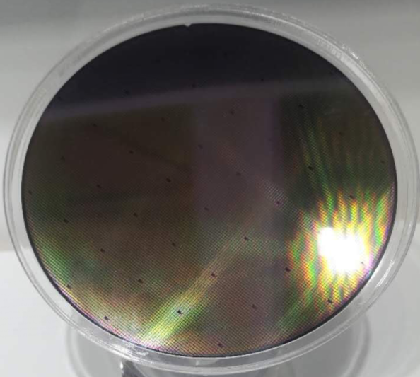
Wafer Epi per diodo laser
Il wafer epitassico LD basato su GaAs, che può generare emissioni stimolanti, è ampiamente utilizzato per la fabbricazione di diodi laser poiché le proprietà superiori del wafer epitassiale GaAs rendono il dispositivo un basso consumo energetico, alta efficienza, lunga durata e così via. Oltre al wafer epitassico LD all'arseniuro di gallio , i materiali semiconduttori comunemente usati sono il solfuro di cadmio (CdS), il fosfuro di indio (InP) e il solfuro di zinco (ZnS).
- Descrizione
Descrizione del prodotto
Xiamen Powerway Advanced Material Co., Ltd (PAM-XIAMEN), un fornitore di wafer epitassiali LD, si concentra sui wafer epi a diodi laser basati su GaAs e InP coltivati dai reattori MOCVD per la comunicazione in fibra ottica, l'applicazione industriale e l'uso per scopi speciali. PAM-XIAMEN è in grado di offrire wafer di epitassia LD basato su substrato GaAs per vari campi, come VCSEL, infrarossi, fotorilevatore e così via. Maggiori dettagli sul materiale del wafer di epitassia LD, fare riferimento alla tabella seguente:
| substrato di materiale | Capacità materiale | lunghezza d'onda | Applicazione |
| GaAs | GaAs / GalnP / AlGaInP / GaInP | 635nm | |
| Wafer in Epi basato su GaAs | 650nm | Laser a emissione di superficie con cavità verticale (VCSEL) RCLED |
|
| GaAs / GalnP / AlGaInP / GaInP | 660nm | ||
| GaAs / AlGaAs / GalnP / AlGaAs / GaAs | 703nm | ||
| GaAs / GalnP / AlGaInP / GaInP | 780nm | ||
| GaAs / GalnP / AlGaInP / GaInP | 785nm | ||
| Wafer in Epi basato su GaAs | 800-1064nm | Infrarossi LD | |
| GaAs / GalnP / AlGaInP / GaInP | 808nm | Infrarossi LD | |
| Wafer in Epi basato su GaAs | 850nm | Laser a emissione di superficie con cavità verticale (VCSEL) RCLED |
|
| Wafer in Epi basato su GaAs | <870nm | Rilevatore di foto | |
| Wafer in Epi basato su GaAs | 850-1100nm | Laser a emissione di superficie con cavità verticale (VCSEL) RCLED |
|
| GaAs / AlGaAs / GaInAs / AlGaAs / GaAs | 905nm | ||
| GaAs / AlGaAs / InGaAs / AlGaAs / GaAs | 950nm | ||
| Wafer in Epi basato su GaAs | 980nm | Infrarossi LD | |
| Epi-wafer basato su InP | 1250-1600nm | Fotorilevatore di valanghe | |
| Wafer in Epi basato su GaAs | 1250-1600nm /> 2.0um (Strato assorbente InGaAs) |
Rilevatore di foto | |
| Wafer in Epi basato su GaAs | 1250-1600nm / <1.4μm (Strato assorbente InGaAsP) |
Rilevatore di foto | |
| Epi-wafer basato su InP | 1270-1630nm | Laser DFB | |
| Substrato GaAsP / GaAs / GaAs | 1300nm | ||
| Epi-wafer basato su InP | 1310nm | Laser FP | |
| Substrato GaAsP / GaAs / GaAs | 1550nm | Laser FP | |
| 1654nm | |||
| Epi-wafer basato su InP | 1900nm | Laser FP | |
| 2004nm |
Informazioni su LD Epitaxy Wafer Applications & Market
Le applicazioni del wafer di epitassia LD basato su GaAs nel campo laser possono essere suddivise in VCSEL e non VCSEL. Le attuali applicazioni di epitassia LD basate su GaAs risiedono principalmente nei VCSEL. VCSEL (Vertical Cavity Surface Emitting Laser), basato su materiali GaAs, viene utilizzato principalmente per il riconoscimento facciale. Si prevede che avrà un alto tasso di crescita in futuro. EEL (Edge Emitting Laser) è un dispositivo non VCSEL, utilizzato principalmente nel campo del lidar automobilistico, e si prevede che la domanda aumenterà con l'espansione del mercato delle auto senza conducente.
Il substrato GaAs utilizzato nel campo laser richiede indicatori tecnici elevati e il prezzo unitario del wafer epitassiale è significativamente superiore a quello di altri campi. Ci si può aspettare il futuro spazio di mercato epitassiale LD. Le applicazioni laser sono le più sensibili alla densità di dislocazione. C'è un elevato requisito per i materiali del substrato GaAs nelle applicazioni laser. Pertanto, il requisito più elevato viene proposto ai produttori di wafer epitassiali LD e al processo di wafer epitassiale LD. Attualmente, il laser a semiconduttore basato su substrato GaAs nella banda del vicino infrarosso (760~1060 nm) ha lo sviluppo più maturo e l'applicazione più diffusa ed è già stato commercializzato.
Nota:
Il governo cinese ha annunciato nuovi limiti all’esportazione di materiali al gallio (come GaAs, GaN, Ga2O3, GaP, InGaAs e GaSb) e materiali al germanio utilizzati per produrre chip semiconduttori. A partire dal 1 agosto 2023, l'esportazione di questi materiali è consentita solo se si ottiene una licenza dal Ministero del Commercio cinese. Spero nella vostra comprensione e collaborazione!
Si prega di vedere sotto le specifiche di dettaglio del wafer di epitassia LD:
Wafer epi con diodo laser da 703 nm
Wafer epi con diodo laser da 780 nm
Wafer epi con diodo laser da 650 nm
Wafer epi con diodo laser 785nm
Wafer epi con diodo laser 808nm-2
Wafer epi con diodo laser da 850 nm
Wafer epi con diodo laser a 905 nm
Wafer epi con diodo laser 950nm
Wafer laser ad alta potenza da 1060 nm
Wafer a diodi laser da 1300 nm
Wafer a diodo laser a pompa da 1460 nm
Wafer epi con diodo laser da 1550 nm
Wafer epi con diodo laser da 1654 nm
Wafer epi con diodo laser 2004nm
GaAs Epitassia con crescita spessa
Struttura Epi basata su GaAs MOCVD sviluppata per emettitore di luce
Stretto InGaAsP Quantum ben cresciuto su wafer InP
Strati InAs Quantum Dot su substrato InP
Wafer laser a cascata quantistica
Chip a emettitore singolo
Chip LD a emettitore singolo 755nm a 8W
Chip LD a emettitore singolo 808nm @ 8W
Chip LD a emettitore singolo 808nm @ 10W
Chip LD a emettitore singolo 830nm @ 2W
Chip LD a emettitore singolo 880nm @ 8W
Chip LD a emettitore singolo 900 + nm @ 10W
Chip LD a emettitore singolo 900 + nm a 15W
Chip LD a emettitore singolo 905nm a 25W
Chip LD a emettitore singolo 1470nm @ 3W
PAM XIAMEN offre chip singolo laser ad alta potenza 1470/1550 nm come segue:
LD Bare Bar
LD Bare Bar per 780nm @ cavità 2,5 mm
LD Bare Bar per 808nm @ cavità 2mm
Barra nuda LD per 808 nm @ cavità 1,5 mm
LD Bare Bar per 880nm @ cavità 2mm
Barra nuda LD per 940 nm @ cavità 2 mm
LD Bare Bar per 940nm @ cavità 3mm
LD Bare Bar per 940nm @ cavity 4mm
Barra nuda LD per 940 nm @ cavità 2 mm
Barra nuda LD per 976 nm @ cavità 4 mm