Silicon carbide has a variety of crystal types, but the silicon crystal structure the market needed is mainly 4H-SiC. So the silicon carbide crystal growth in crystal types is a defect. To a certain extent, it can be distinguished by the naked eye. A more accurate measurement method for testing the silicon carbide crystal distribution is Raman spectroscopy: Raman spectroscopy has characteristics for crystals, and the peak positions of the light emitted by different crystals are different.
1. What is Raman Spectroscopy?
Nel 1928, lo scienziato indiano Raman scoprì lo scattering Raman nell'esperimento di studio dello spettro di scattering del benzene liquido. La spettroscopia di scattering Raman, in termini semplici, è che usa un fascio di luce incidente su una sostanza, la frequenza della luce incidente è v e la frequenza della luce diffusa risultante sarà v, v + Δv1, v-Δv1, v + Δv2, v-Δv2 e così via. Questi Δv1, Δv2, ecc. Δv sono con caratteristiche. In altre parole, ogni sostanza ha una certa differenza (posizione del picco, intensità di picco), che è chiamata spostamento Raman (la luce emessa meno la luce incidente).
Ad esempio, lo spettro Raman di 4H-SiC è:
| Spostamento Raman (cm-1) | Onda acustica trasversale E2 | Onda acustica trasversale E2 | Onda acustica trasversale A1 | Onda acustica trasversale E2 | Onda acustica trasversale A1 | Onda acustica longitudinale A1 | LOPC | LOPC |
| 4H-SiC | 194.958 | 204.034 | 610.031 | 776.489 | 796.861 | 963.106 | 964.769 | 994.643 |
The table above shown here is the Raman shift. During the silicon carbide crystal distribution measurement, the computer will help to calculate it and process it as a Raman shift spectrum.
2. How to Test the Silicon Carbide Crystal Distrubution?
Le condizioni di test tipiche sono: utilizzando il laser a 532 nm del laser Ar + dello spettrometro LabRAM HR Raman, è incidente verticalmente, la potenza di eccitazione è di 200 mW e la modalità di raccolta della luce diffusa è la modalità di retrodiffusione. La luce incidente con diverse lunghezze d'onda ha diverse profondità di penetrazione. In generale, il laser a 266 nm è 0,2 um, il laser a 325 nm è 2 um e il laser a 514 nm è 30 um, il che significa che la luce ultravioletta può essere utilizzata solo per misurare campioni sottili.
Because the silicon carbide wafer has different positions, multiple measurements will be taken to obtain the silicon carbide crystal distribution:
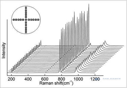
The data has three indicators: the position of the peak, the height of the peak (light intensity), and the width of the peak. Only when the peak position is completely matched, can it be il 4H-SiC qualificato. Come con XRD, ogni volta che ci sono altri picchi, sono sostanze di altre fasi, il che è un difetto.
The difference in the position of the peak is due to the difference in the energy of the phonons brought about by the different silicon carbide crystal lattices, that is, the different frequencies. Each phonon has its corresponding energy level. The virtual energy level theory can be used to explain Raman (non-linear process):
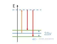
La particella assorbe la luce incidente al livello di energia virtuale (arancione), quindi torna a un livello di energia vibrazionale (rosso) diverso dal livello di energia originale. Poiché il livello di energia superiore è un livello di energia virtuale, la frequenza della luce incidente può essere variata, purché non sia in conflitto con il livello di energia reale originale.
Vale la pena notare che la modalità LOPC (964,769 cm-1) può essere utilizzata per analizzare la concentrazione del vettore:
n = 1.25 * 1017cm-2 *(964.769cm-1-VLOPC measurement)
As the carrier concentration increases, the interaction between atoms and the lattice increases, which makes the Raman peak blue shift (smaller), the intensity decreases, and the width increases. This method is not as accurate as other methods and can only be used as an aid to analyze the silicon carbide crystal distribution.
3. Why not Use XRD to Measure Silicon Carbide Crystal Distribution?
X-rays are optical radiation generated by the transition of electrons in the inner layer of atoms under the bombardment of high-speed moving electrons, including continuous X-rays and characteristic X-rays. Silicon carbide single crystal can be used as X-ray gratings, and the coherent scattering produced by these large numbers of particles (atoms, ions, or molecules) will cause light interference, increasing or decreasing the intensity of scattered X-rays. Due to the superposition of scattered waves from a large number of particles, the beams that interfere with each other to produce the highest intensity are called X-ray diffraction lines.
Per soddisfare le condizioni di diffrazione, è possibile applicare la formula di Bragg: 2dsinθ = nλ.
Il raggio incidente fa sì che ogni diffusore irradi nuovamente una piccola parte della sua intensità come un'onda sferica. Se gli scatterer sono disposti simmetricamente con l'intervallo d, queste onde sferiche saranno sincronizzate solo nella direzione in cui la loro differenza di lunghezza del percorso 2dsinθ è uguale a un multiplo intero della lunghezza d'onda λ. In questo caso, una parte del raggio incidente viene deviata di un angolo di 2θ, che produrrà punti di riflessione nel modello di diffrazione.
Use X-rays of known wavelengths to measure the θ angle to calculate the interplanar spacing d, which is used for X-ray structure analysis; the other is to use a silicon carbide seed crystal with a known d to measure the θ angle to calculate the characteristic X-ray wavelength, and then the elements contained in the sample can be found in the existing data.
The measurement formula is 2dSinθ=λ. While the d value among the cubic silicon carbide crystal is close, and the characteristic is not obvious enough, the accurate silicon carbide crystal distribution cannot be precisely determined. For these reasons, it is not suitable to use the XRD to measure the distribution of silicon carbide crystals.

Per ulteriori informazioni, contattaci tramite e-mail all'indirizzo victorchan@powerwaywafer.com e powerwaymaterial@gmail.com.