Indium arsenide (InAs) single crystal is available with S doped, Zn doped, Sn doped and undoped conductivity types in various orientations and sizes. InAs is a compound semiconductor material that is difficult to purify. Indium arsenide single crystal growth can be processed by LEC method and VGF method. The single crystal ingot of InAs has a high electron mobility and mobility ratio (μe/μh=70), and is widely used in IR photodiode semiconductors, and is proposed as a composition for infrared lasers and terahertz oscillators. See the following part for specific parameters:

1. Specifications of Indium Arsenide Single Crystal
|
InAs Single Crystal |
|
| Item | Parameter |
| Orientation | (100), (110), (111) |
| Diameter | (40~100) ± 1mm |
| Length | >50mm |
| EPD | A <5000 cm-2, B<5 x 104 cm-2 |
| Purity | 99.9999% |
| Conductivity Type | N-type, Undoped, P-type |
| Edge surface finishing | Cylindrical ground |
| Growth Method | VGF, LEC |
2. Indium Arsenide Properties
The bulk indium arsenide is a narrow direct-band-gap with a cubic zinc blende structure and a lattice constant a = 6.058 Å, which belongs to III-V semiconductor compound material. The InAs band gap is 0.35 eV. The residual carrier concentration of the undoped InAs ingot is higher than 1×10¹⁶/cm3, the room temperature electron mobility is 3.3×104cm2/(V·s), and the hole mobility is 460cm2/(V·s). The effective segregation coefficient of sulfur in InAs is close to 1, so it is used as an n-type dopant to improve the uniformity of the longitudinal carrier concentration distribution. Industrial InAs(S) single crystal, n≥1×10¹⁷/cm3, μ≤2.0×104cm2/(V·s), EPD≤5×10⁴/cm2.
| Physical Properties | |
| Chemical formula | InAs |
| Molar mass | 189.740 g/mol |
| Density | 5.67 g/cm3 |
| Melting point | 942 °C (1,728 °F; 1,215 K) |
| Band gap | 0.354 eV (300 K) |
| Electron mobility | 40000 cm2/(V*s) |
| Thermal conductivity | 0.27 W/(cm*K) (300 K) |
| Refractive index(nD) | 3.51 |
| Structure | |
| Crystal structure | Zinc Blende |
| Lattice constant | a = 6.0583 Å |
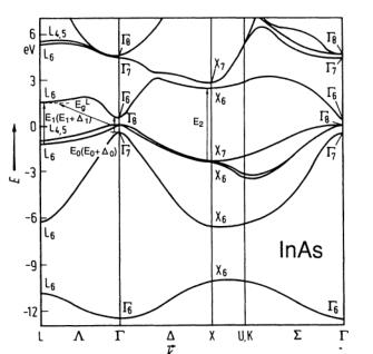
The diagram shows the InAs electronic energy and band structure.
From the following Fig of indium arsenide crystal structure, we can see that the InAs unit cell is composed of four In atoms and four As atoms. In the structure, the anions of as coordinate with the four cations of In to form an AsIn 4 tetrahedron with four As-In bonds.

InAs Structure
3. Comparison between the LEC-InAs Single Crystal and VGF-InAs Single Crystal
The research is carried out for studying the LEC-InAs and VGF-InAs by infrared transmission and reflection spectroscopy, double crystal X-ray diffraction, low-temperature photoluminescence spectroscopy and Hall Effect measurements. Compared with the Indium Arsenide single crystal grown by LEC, the InAs single crystal grown by VGF has lower concentration of native defects, making it better electrical and optical properties. In addition, the X-ray rocking curve shows a narrower FWHM of VGF-InAs single crystal than that of LEC-InAs single crystal, which indicates better lattice perfection of VGF-InAs single crystal.
Since the indium arsenide nano crystals provide good basis for commercial applications and new technologies, there are lots of researches on indium arsenide refractive index and optical absorption. InAs wafer made from the ingot is ideal for fabricating electronic and optoelectronic devices, such as transistor, photodetectors and lasers.

For more information, please contact us email at victorchan@powerwaywafer.com and powerwaymaterial@gmail.com.