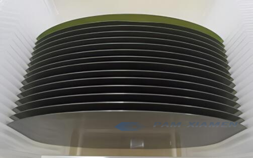
Epitaxial InGaAsP / InP photodiode wafer is offered for making InP-based optoelectronic devices. For such devices, InGaAsP quaternary material is commonly grown on InP substrate as ohmic contact layers. Quaternary InGaAsP thin film epitaxial on InP is sensitive to InP luminescence. InGaAsP / InP PIN photodiode structure can make the devices with low leakage current. The details of GaInAsP / InP heterojunction photodiode structure from PAM-XIAMEN is as follows:

1. InGaAsP Photodiode Structure
| 1550nm Epi Structure of Photodiode Based on GaInAsP / InP for PIN (PAM211119-1550PIN) | |||||
| Layer | Material | Thickness(nm) | Dopant | Dopant Concentration(cm-3) | Type |
| 4 | GaxIn1-xAsyP1-y | – | Si | – | N |
| 3 | InP | – | Si | – | N |
| 2 | GaxIn1-xAs | – | Undoped | – | N |
| 1 | InP | 0.5-1 | Si | – | N |
| N+ InP Substrate | |||||
Remarks:
1) Lattice-matching compounds of InGaAsP allow composition of absorber and transparent layers;
2) InGaAsP / InP characteristics include bandgap variation between 1.65 μm and 0.92 μm, depending on InGaAsP composition and absorption constant of In0.53Ga0.47As at 1.55 μm about 7,000 cm-1.
2. Determination of Refractive Index of InGaAsP / InP Structure Epitaxial Layer
For devices fabricated on InGaAsP / InP quaternary avalanche photodiode structure, the parameters of the epitaxial layer are not only determined by the ratio of each component before epitaxy but also closely related to the epitaxial process. Therefore, it is necessary to ensure that the device meets the predetermined design requirements from the process and improve the consistency of the process, and it is also necessary to sample the parameters of the epitaxial layer for a certain period of time.
The direct determination of the refractive index of the epitaxial layer of the InGaAsP / InP heterostructure PIN photodiode is to couple the Ar+ laser into the epitaxial layer through the etched grating on the epitaxial layer, and the fluorescence emitted by the Ar+ fluoride is then coupled out by the grating. The main disadvantage of the method that the refractive index and thickness of the epitaxial layer can be obtained by calculation is that an etched grating needs to be fabricated on the epitaxial layer, and the calculation is obtained under the assumption that the depth of the grating groove is 0.1 μm in advance, so the obtained refractive index accuracy of InGaAs / InGaAsP / InP structure is low, only around ±0.01.
3. FAQ for PIN Photodiode Wafer
Q: May I know if you have the data of the refractive index of the MQW layer in 1550nm PIN photodiode structure?
A: The refractive index of this PIN photodiode wafer is around XX between 1000nm-1600nm, and it has small fluctuation. Please contact our sales team victorchan@powerwaywafer.com for specific value.
For more information, please contact us email at victorchan@powerwaywafer.com and powerwaymaterial@gmail.com.

