PAM-XIAMEN offers PSS patterned sapphire substrate for high brightness GaN based LED EPI growing application. The patterned sapphire substrate wafer è far crescere una maschera di incisione a secco sul substrato di zaffiro. La maschera è incisa mediante un processo di fotolitografia standard. Quindi, lo zaffiro viene inciso con la tecnologia di incisione ICP e nel frattempo la maschera viene rimossa. Successivamente, il materiale GaN viene fatto crescere sullo zaffiro, in modo che l'epitassia verticale del materiale GaN diventi l'epitassia orizzontale. I dettagli del substrato in zaffiro modellato sono di seguito:
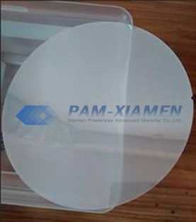
Substrato Zaffiro PSS
1.Specificaziones di Substrato di zaffiro modellato
| Parametri | Specificazione | Unità |
| Materiale | Monocristallino di elevata purezza Al2O3 | |
| Diametro | 50,8 ± 0,1 | ㎜ |
| Spessore | 430 ± 10 | ㎛ |
| Variazione totale dello spessore | ≤10 | ㎛ |
| Lunghezza piatta primaria | 16,0 ± 1,0 | ㎜ |
| Orientamento piatto primario | Un piano ± 0,2 | |
| Qualità della superficie frontale | Pronto per l'epitassia | |
| Rugosità della superficie posteriore | 1.0 ± 0.1 | ㎛ |
| Orientamento della superficie A | 0˚off ± 0,1 | |
| Orientamento della superficie M | 0,2˚off ± 0,10 | |
| Orientamento della superficie R | R9 | |
| ARCO | -10 ~ 0 | ㎛ |
| ORDITO | ≤15 | ㎛ |
| Larghezza motivo | 2,7 ± 0,15 | ㎛ |
| Altezza del motivo | 1,7 ± 0,15 | ㎛ |
| Passo del modello | 3,0 ± 0,05 | ㎛ |
2.Perché scegliere il substrato in zaffiro modellato per LED?
On the one hand, the cone-shaped patterned sapphire substrate wafer can effectively reduce the dislocation density of the GaN epitaxial material(the patterned sapphire substrate dislocation is low), thereby reducing the non-radiative recombination of the active area, reducing the reverse leakage current, and improving the life of the LED. On the other hand, the light emitted from the active region is scattered multiple times by the interface of GaN and sapphire substrate, and the exit angle of total reflection light is changed, increasing the probability that the light of the flip-chip LED emerges from the sapphire substrate, thereby improving the extraction efficiency of the light.
In sintesi, la luminosità della luce emessa dal LED cresciuto sul substrato in zaffiro con motivo nanometrico è notevolmente migliorata rispetto a quella del LED tradizionale. La corrente di dispersione inversa viene ridotta, allungando la vita del LED.
A patterned sapphire substrate belongs to the semiconductor industry. As a high-brightness epitaxial material, it is the source material of the LED lighting industry. Meanwhile, using PSS Al2O3 wafer to grow epitaxial wafers is the most effective way to improve the brightness of the chip. It is also the best choice for the high-power and high-brightness epitaxial wafers.

Per ulteriori informazioni, contattaci tramite e-mail all'indirizzo victorchan@powerwaywafer.com and powerwaymaterial@gmail.com.