窒化物の1.1Crystal構造
III族窒化物は、結晶構造のものとすることができる:ウルツ鉱(Wzと)、閃亜鉛鉱(ZB)、
そして、塩を揺すります。 周囲条件の下では、熱力学的に安定な構造があります
バルクのAlN、GaN系、およびインのウルツ鉱。 GaN及びInNのための閃亜鉛鉱構造を持っています
立方晶の{0 1}結晶面上の薄膜のエピタキシャル成長により安定化されて
Si等の基板[1]、SiCの[2]、酸化マグネシウム[3]、及びGaAs [4]。 このような場合には、固有
Wzと構造を形成する傾向は、トポロジカルな互換性によって克服されます。
しかし、Wzと構造が非常に高い拡張欠陥部位に存在することができます。 ザ・
岩塩形だけで、高圧力下で可能であり、そのため、実験室のフォームです
運動の。
私たちは今、窒化物の様々な形のための空間群を議論してみましょう。 岩塩、
または塩化ナトリウム、theHermann・モーガン表記で空間群Fm3m有する構造(及び
O5
シェーンフリース記号におけるh)は非常に高いの下でのAlN、GaN系、及びイン誘導することができます
圧力。 この理由は、格子寸法の減少が生じることがあります
interionicクーロン相互作用は、共有結合、自然の上にイオン性を支持します。 ザ・
塩構造をロックするための構造的な相転移を実験的に観察されました
推定された圧力値以下のAlNため22.9GPa(他の見積りの17 GPA)[5]
GaN系のため52.2GPa [6]、及びイン12.1GPa [7]。 岩塩III窒化物にすることはできません
任意のエピタキシャル成長によって生成さ。
閃亜鉛鉱構造のためのスペースのグループ化はHermann-でF43mです
モーガン表記とT2D
シェーン表記インチ 閃亜鉛鉱構造を持っています
4つのIII族元素と4つの窒素元素を含む立方単位セル。
(用語亜鉛鉱は、可能性のZnSなどの化合物に由来するが
立方または六方晶相であること、それは、化合物のために普遍的に使用されてきました
立方対称性を有する半導体。 以下のために使用されるべき正しい用語
GaNのキュービック相は、実際には閃亜鉛鉱です。 しかし、用法と一致するように
文学を通して、でも精度を犠牲にし、長期閃亜鉛鉱があり
)このマニュアルで使用されて。 単位セル内の原子の位置が同一であります
ダイヤモンドの結晶構造。 両方の構造は、二つの相互浸透facecenteredから成り
立方副格子は、対角線本体に沿った距離の四分の一により一部相殺されました。
四面体の中心に位置するような構造中の各原子は、見ることができます
その4人の最も近い隣人が四面体の四隅を定義しています。 ザ・
stacking sequence for the (1 1 1) close-packed planes in this structure is AaBbCc.
Lowercase and uppercase letters stand for the two different kinds of constituents.
The wurtzite structure has a hexagonal unit cell and thus two lattice constants, c
and a. It contains six atoms of each type. The space grouping for the wurtzite
structure is P63mc in the Hermann–Mauguin notation and C46
v in the Schoenflies
notation. The point group symmetry is 6mm in the Hermann–Mauguin notation
and C6v in the Schoenflies notation. The Wz structure consists of two interpenetrating
hexagonal close-packed (hcp) sublattices, each with one type of atom, offset along
the c-axis by 5/8 of the cell height (5c/8). The wurtzite and zinc blende structures are
somewhat similar and yet different. In both cases, each group III atom is coordinated
by four nitrogen atoms. Conversely, each nitrogen atom is coordinated by four group
III atoms. The main difference between these two structures lies in the stacking
sequence of closest packed diatomic planes. The Wz structure consists of alternating
biatomic close-packed (0 0 0 1) planes of Ga and N pairs, thus the stacking sequence of
the (0 0 0 1) plane is AaBbAa in the (0 0 0 1) direction.
Although the main interest is in Wz GaN as opposed to zinc blende GaN, a
description of stacking sequence of both GaN polytypes with the accepted Ramsdel
notation is warranted, so is the stacking order of SiC polytypes that are relevant to
GaN because they are used for substrates in GaN epitaxy. Therefore, a generic
description of stacking in Wz semiconductors is given below. A comprehensive
description of the tetrahedrally coordinated structures is imperative for a clear picture
of nitride semiconductors, particularly the extended defects that are discussed in
detail in Chapter 4. The bonds describe a tetrahedron denoted by T, which has one
atom species at each of the three corners and the other atom species in its center [8,9].
The basal plane of this structure is defined by one face of the tetrahedron and the
bond perpendicular to this plane defines the c-axis. A rotation of 180 around the caxis
produces a twin variant denoted by T0 as shown in Figure 1.1a (left).

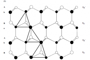
Figure 1.1 Representation of the tetrahedrally coordinated
materials in the Ramsdel notation. (a) The two possible
tetrahedra. (b) The T1, T03
, T1, T03
, tetrahedral stacking composing
the 2H sequence. Courtesy of Pierre Ruterana [9].
about one of the {1 1 0 0} m-planes. A tetrahedron can occupy one of the three
possible positions in the basal plane. The representation of the tetrahedrally
coordinated materials in the Ramsdel notation is shown in Figure 1.1a for two
possible tetrahedra, one is the mirror image twin of the other with respect to the
(1 1 0 0) m-plane. The single bonds are on the (1 1 2 0) plane, called the a-plane. The
layers of the tetrahedra can then be denoted by T1, T2, T3, and by T01
; T02
; T03
for its
twin. An example of T1; T0; T1; T03
stacking order representing 2H ordering as in
wurtzitic GaN is shown in Figure 1.1b. The structure of nitride semiconductors and
most relevant polytypes of SiC can be completely described by a combinatorial
stacking of the aforementioned six tetrahedra layers. Naturally, not all the stacking
sequences must obey the following two rules to keep a corner sharing structure, as
such not all stacking orders are allowed:
(i) A tetrahedron T can be followed by another one of the same kind with the
following subscript: T1T2T3, and inversely for the twin variant: T03
T02
T01
.
(ii) A tetrahedron T1 must be followed by the twin variant of the preceding subscript:
T1T03
, and inversely for its twin variant: T01
T2.
In the Ramsdel notation, the stacking order for the wurtzite structure corresponding
to various polytypes can be denoted as
. T1T03
or T2T01
or T3T02
for the 2H polytype, which is also applicable to Wz nitride
semiconductors;
. T1T2T01
T03
for the 4H polytype;
. T1T2T3T02
T01
T03
for the 6H polytype;
. T1T2T3 or T03
T02
T01
for the 3C polytype.
The 3C, 4H, and 6H stacking sequences as well as 2H sequence on 6H sequence are
discussed in Chapter 3.
Recall that GaN crystallizes in the cubic structure (zinc blende or sphalerite, the
latter being the correct term and the former being the one used universally) or in the
more stable hexagonal structure (wurtzite). The anions (N3) form an hcp structure
in which the cations (Ga3þ) occupy half of the tetrahedral sites. The structure of a unit
cell of GaN projected along [0 0 0 1] is depicted schematically in Figure 1.2. The open
symbols represent g sites that are occupied by nitrogen atoms; theGa atoms are in the
tetrahedral sites, b. These latter sites can either be at heights (3/8)c above (b1) or below
(b2) N site, depending on the crystal polarity.
A stick-and-ball representation of Ga-polarity and N-polarity Wz structure is
depicted in Figure 1.3. The Wz and zinc blende structures differ only in the bond
angle of the second nearest neighbor (Figure 1.4). As clearly shown, the stacking
order of theWz along the [0 0 0 1] c-direction is AaBb, meaning a mirror image but no
in-plane rotation with the bond angles. In the zinc blende structure along the [1 1 1]
direction, there is a 60 rotation that causes a stacking order of AaBbCc. The point
with regard to rotation is illustrated in Figure 1.4b. The nomenclature for various
commonly used planes of hexagonal semiconductors in two- and three-dimensional
versions is presented in Figures 1.5 and 1.6. The Wz group III nitrides lack an
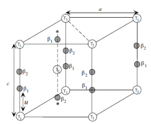
Figure 1.2 Schematic diagram showing the b1 and b2 tetrahedral
sites of GaN unit cell. Starting with the assumption that N
occupies the g sites, only one family of b sites can be
simultaneously occupied by Ga atoms. Courtesy of Pierre
Ruterana [9].
inversion plane perpendicular to the c-axis; thus, nitride surfaces have either a group
III element (Al, Ga, or In) polarity (referred to as Ga-polarity) with a designation of
(0 0 0 1) or (0 0 0 1)A plane or a N-polarity with a designation of (0 0 0 1) or (0 0 0 1)B
plane.We will use the former notations for each. The distinction between these two
directions is essential in nitrides because of their implications for the polarity of the
polarization charge. Three surfaces and directions are of special importance in
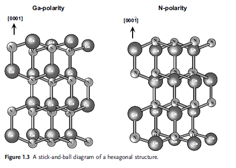
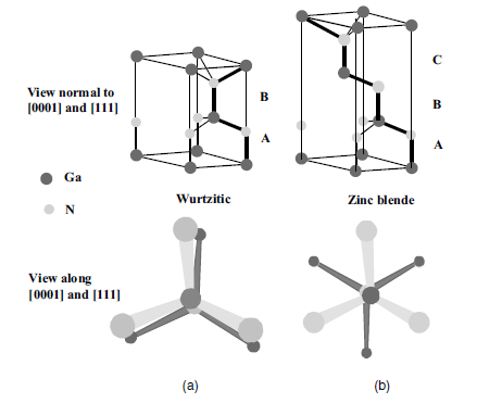
Figure 1.4 A stick-and-ball stacking model of
crystals with (a, both top and bottom) 2H
wurtzitic and (b, both top and bottom) 3C
zinc blende polytypes. The bonds in an A-plane
(1 1 2 0) are indicated with heavier lines to
accentuate the stacking sequence. The figures on
top depict the three-dimensional view. The
figures at the bottom indicate the projections on
the (0 0 0 1) and (1 1 1) planes for wurtzitic and
cubic phases, respectively. Note the rotation in
the zinc blende case along the h1 11i direction.
(Please find a color version of this figure on the
color tables.)
nitrides, which are (0 0 0 1) c-, (1 1 2 0) a-, and (1 1 0 0) m-planes and the directions
associated with them, h00 01i, h1120i, and h1100i as shown in Figure 1.7. The
(0 0 0 1), or the basal plane, is the most commonly used surface for growth. The other
two are important in that they represent the primary directions employed in
reflection high-energy electron diffraction (RHEED) observations in molecular beam
epitaxial growth, apart from being perpendicular to one another. They also represent
the direction of stripes employed in the epitaxial lateral overgrowth (ELO), details of
which are discussed in Section 3.5.5.2.
The cohesive energy per bond in the wurtzite form is 2.88 eV (63.5 kcal mol1),
2.2 eV (48.5 kcal mol1), and 1.93 eV (42.5 kcal mol1) for AlN, GaN, and InN,
respectively [10]. The calculated energy difference DEW-ZB between wurtzite
and zinc blende lattice is small [11]: DEW-ZB¼18.41 meV/atom for AlN,
DEW-ZB¼11.44 meV/atom for InN, and DEW-ZB¼9.88 meV/atom for GaN.
Wurtzite form is energetically preferable for all three nitrides compared to zinc
blende, although the energy difference is small.
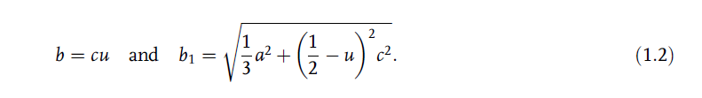
TheWzstructure can be represented by lattice parameters a in the basal plane and c
in the perpendicular direction, and the internal parameter u, as shown in Figure 1.8.
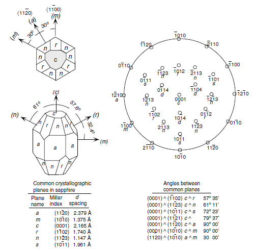
Figure 1.5 Labeling of planes in hexagonal symmetry ( for sapphire).
The u parameter is defined as the anion–cation bond length (also the nearest
neighbor distance) divided by the c lattice parameter. The c parameter depicts the
unit cell height. The wurtzite structure is a hexagonal close-packed lattice, comprising
vertically oriented X–N units at the lattice sites. The basal plane lattice
parameter (the edge length of the basal plane hexagon) is universally depicted by a
and the axial lattice parameter, perpendicular to the basal plane, is universally
described by c. The interatomic distance in the basic unit is described by the
internal parameter u. In an ideal wurtzite structure represented by four touching
hard spheres, the values of the axial ratio and the internal parameter are
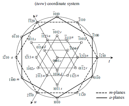
Figure 1.6 A magnified view of labeling of planes
in hexagonal symmetry in the (tuvw) coordinate
system with w representing the unit vector in the
c-direction. The lines are simply to show
thesymmetryonly. If thelinesconnectingm-points
among each other and a-pointsamong each other
were to be interpreted as the projection of those
planes on the c-plane, the roles would be switched
in that the lines connecting the m-points would
actually represent the a-planes and lines
connecting the a-points would actually represent
the m-planes that are normal to the plane of the
page.
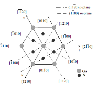
Figure 1.7 The orientations which are commonly used in nitrides,
namely the (1 1 2 0) and (1 1 0 0) planes and associated directions
are shown as projections on the (0 0 0 1) basal plane.
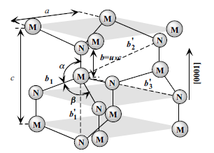
Figure 1.8 Schematic representation of a wurtzitic metal nitride
structure with lattice constants a in the basal plane and c in the
basal direction, u parameter, which is expressed as the bond
length or the nearest neighbor distance (b) divided by c (0.375
in ideal crystal), a and b (109.47 in ideal crystal) are the bond
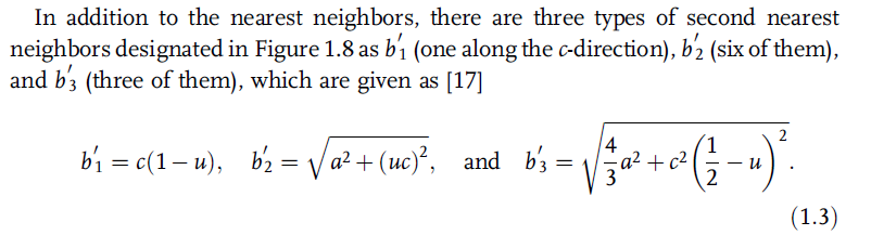
angles, and b01, b02, and b03, represent the three types of second
nearest neighbor distances.
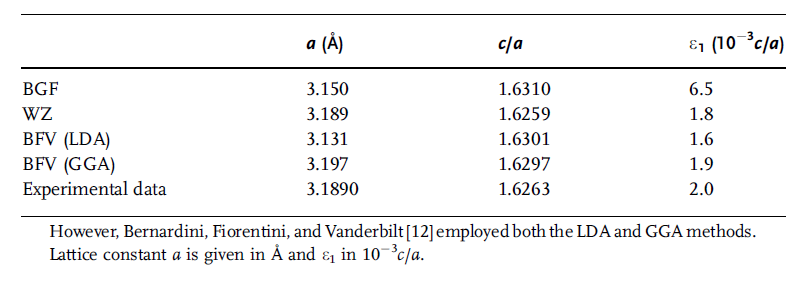
approximation (GGA) and local density approximation (LDA). The experimental data
are from Leszczynski et al. [15].
In all Wz III nitrides, experimentally observed c/a ratios are smaller than ideal and
it has been postulated that not being so would lead to the zinc blende phase [16]. There
are two avenues that can lead to a deviation from ideal: changing the c/a ratio or
changing the u value. It should be pointed out that a strong correlation exists between
the c/a ratio and the u parameter so that when c/a decreases, the u parameter
increases in a manner to keep the four tetrahedral distances nearly constant through a
distortion of tetrahedral angles. For equal bond length to prevail, the following
relation must hold:![]()
Table 1.1 Structural parameters for GaN reported by Bechstedt,
Großner, and Furthm€uller (BGF) [13] and by Wei and Zunger
(WZ) [14] using the local density approximation (LDA).
The nearest neighbor bond length along the c-direction (expressed as b in
Figure 1.8) and off c-axis (expressed as b1 in Figure 1.8) can be calculated as
The bond angles, a and b, are given by [17]
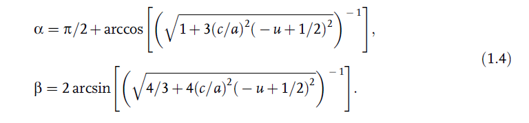
Table 1.2 tabulates the calculated as well as experimentally observed structural
parameters discussed above, inclusive of the lattice parameters, the nearest and
second nearest neighbor distances, and the bond angles for three end binaries, GaN,
AlN, and InN. The distances are in terms of Å.
The lattice parameters are commonly measured at room temperature by X-ray
diffraction (XRD), which happens to be the most accurate one, using the Bragg law. In
ternary compounds, the technique is also used for determining the composition;
however, strain and relevant issues must be accounted for as the samples are in the
Table 1.2 Calculated (for ideal crystal) and experimentally
observed structural parameters for GaN, AlN, and InN [17].

form of epitaxial layers on foreign substrates. The accuracy of X-ray diffraction and
less than accurate knowledge of the elastic parameters together allow determination of
the composition to only within about 1% molar fraction. In addition to composition,
the lattice parameter can be affected by free charge, impurities, stress (strain), and
temperature [18]. Because the c/a ratio correlates with the difference of the electronegativities
ofthetwoconstituents,componentswiththe greatestdifferencesshowthe
largest departure from the ideal c/a ratio [19]. ForGaN, the c/a ratio and the value of u
are measured as 1.627 (1.634 in Ref. [17]) and 0.377, respectively, which are close to the
ideal values [20]. AlN deviates significantly from the ideal parameters: c/a¼1.601
(1.606 in Ref. [17])andu¼0.382.Althoughthe data forInNare notas reliable, values of
u¼0.379 and c/a¼1.601 have been reported [17]. Inhomogeneities, strain, partial
relaxation of strain, and high concentration of structural defects may distort the lattice
constants from their intrinsic values and cause a wide dispersion among the reported
values. Table 1.3 lists a comparison of measured and calculated lattice parameters
reported for AlN,GaN, and InN crystallized in the wurtzite structure in more detail in
terms of the specifics of the sample used for measurements and complements. The
dispersion is even a greater concern in ternary and quaternaries, as compositional
inhomogeneities, in addition to the aforementioned issues, cause an additional
dispersion. The particulars of the ternaries are discussed in Section 1.5.
The wurtzite polytypes of GaN, AlN, and InN form a continuous alloy system
whose direct bandgaps range, according to data that adorned the literature for years,
from 1.9 eV for InN, to 3.42 eV for GaN, and to 6.2 eV for AlN. A revisit of the InN
bandgap indicates it to be about 0.78 eV [30] and the same for AlN is about 6 eV in
which case the energy range covered would be about 0.7–6 eV. Thus, the III–V
nitrides could potentially be fabricated into optical devices, which are active at
wavelengths ranging from the red well to the ultraviolet. The bandgaps of nitrides,
Table 1.3 Measured and calculated lattice constants of wurtzite AlN, GaN, and InN.
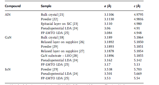
LDA: local density approximation; FP-LMTO: full-potential linear muffin–tin orbital.
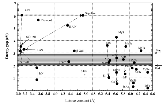
Figure 1.9 The bandgaps of nitrides, substrates commonly used
for nitrides, and other conventional semiconductors versus
their lattice constants. (Please find a color version of this figure
on the color tables.)
substrates commonly used for nitrides, and other conventional semiconductors are
shown in Figure 1.9 with respect to their lattice constants.
All III nitrides have partially covalent and partially ionic bonds. The concept of
fractional ionic character (FIC) is useful in interpreting many physical phenomena in
the crystals [31,32]. The FIC may be defined for a binary compound AB as
FIC ¼ jQA QBj=jQA þQBj, where QA and QB are effective charges on atoms A
and B. The FIC values range from zero for a covalent compound (each atom has four
electrons) to 1 for an ionic compound (all eight electrons belong to the anion).
Figure 1.10 displays the charge distribution along the AB bond for all three compounds.
The arrow along the bond charge indicates the atomic boundaries in the
crystals that are not always at the minimumof the line charge along the bond AB. This
should be expected taking into account the partial covalent bond of the compounds,
because only in the ionic crystals, the atomic boundary is clearly defined.Table 1.4 lists
the calculated effective radii, rIII and rN, the effective charges, and FIC for AlN, GaN,
and InN.Theionicity ofAlNis high. Thismayexplain the difficulties withAlNdoping.
It is well known that only covalent semiconductors or semiconductors with a large
covalent component can form hydrogen-like shallow levels in the bandgap by
substitution of a host atom with a neighbor with one more or one less electron. GaN
and InN have a smaller than AlN but nearly equal ionicity.GaN was doped both p- and
n-type. Thus, one can expect that InN can also be doped n- and p-type. To date, only
n-type InN has been obtained because of high volatility of nitrogen and easiness of
nitrogen vacancy formation that acts as a donor in this compound.
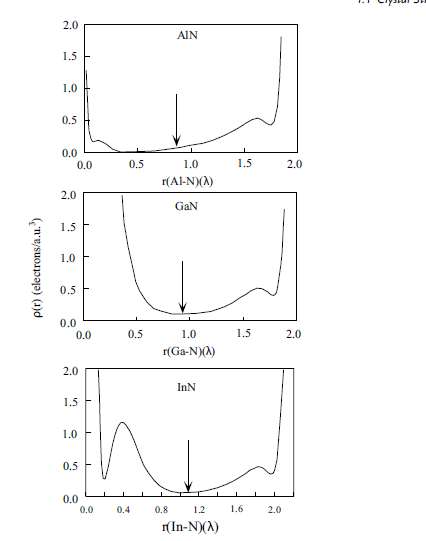
Figure 1.10 Charge density along the III–N bond in III nitride semiconductors
The III-nitrides are commonly grown on mismatched substrates because of the lack
of suitable native substrates. Thus, the epitaxial layers are strained during cool down, if
they are sufficiently thick for themto relax at the growth temperature. The mechanical
forces related to strain dramatically change the band structure of the epitaxial layers.
The pressure dependence of the bandgap energy Eg can be expressed as Eg¼Eg(0)
gPþdP2, where Eg(0) is the bandgap of stress-free semiconductor, g and d are the
Table 1.4 Calculated ionic radii (Å), effective charges (electrons),
and the fractional ionic character (FIC) for III nitrides [32].
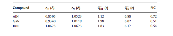
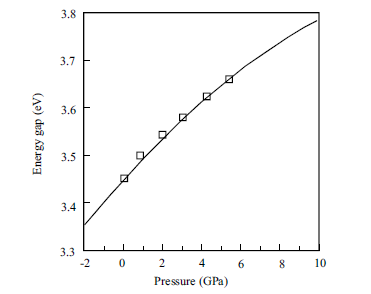
Figure 1.11 Pressure dependence of the GaN energy gap,
showing the typical sublinear character. Solid line represents the
calculations of Christiansen and Gorczyca [35], which have been
rigidly upshifted by 0.82 eV for a better fit with experiments,
and the squares represent experimental results [6].
and1.8 · 105, respectively [33,34].The bandgap is in termsof eVand the pressure is
in terms of kbar. The pressure dependence has, in general, a sublinear character. The
variation of the GaN energy gap with pressure, both theoretical [35] and experimental
[6], is shown in Figure 1.11. The calculated pressure coefficients for III nitrides are
given in Table 1.5.
Parameters associated with mechanical properties of GaN in wurtzitic phase are
tabulated in Tables 1.6 and 1.7, the latter dealing with the sound wave velocity. The
same parameters for the zinc blende phase ofGaN are tabulated in Tables 1.8 and 1.9.
Table 1.5 Calculated pressure coefficients for III nitrides including
wurtzitic, zinc blende, and rock salt phases (g in units of
meV GPa1 and d in units of meV GPa2) [35].
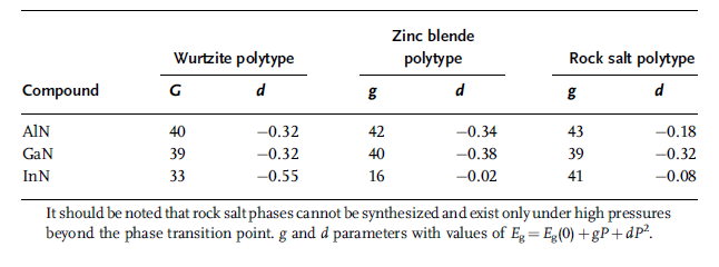
Table 1.6 Parameters related to mechanical properties of wurtzitic GaN (in part after Ref. [36]).

Table 1.7 Wave propagation properties in wurtzitic GaN [36].
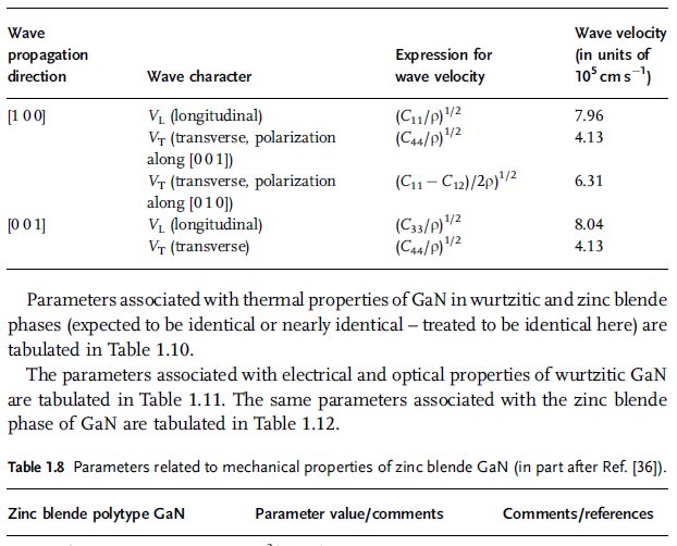

Table 1.9 Wave propagation properties in zinc blende GaN (after Ref. [36]).
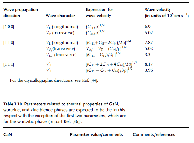

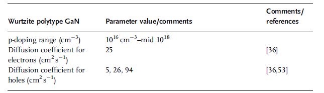
Table 1.11 Parameters related to electrical and optical properties
of Wz GaN (in part after Refs [36,44]).


Table 1.11 (Continued)
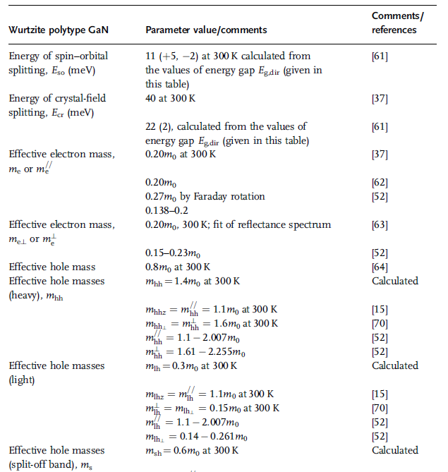

Table 1.11 (Continued)
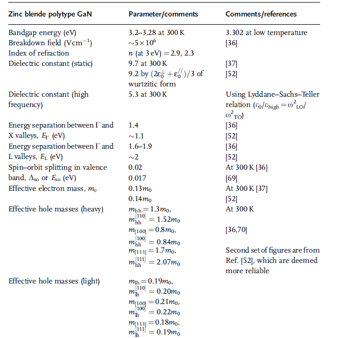
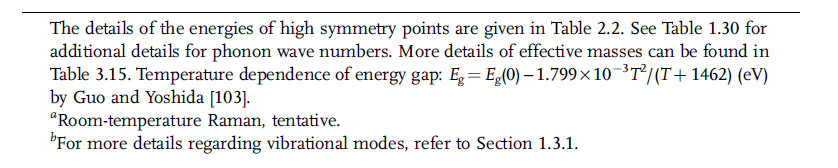
The phonon energies are discussed later on in Table 1.27 in detail and effective
masses are discussed in Chapter 2. More details of effective masses can be found in
Table 2.9.
More should be said about the dielectric constants. Electromagnetic theory indicates
that for any longitudinal electromagnetic wave to propagate, the dielectric function
e(o) must vanish. Doing so leads to [66]
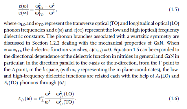
Likewise, Equation 1.5 can be expanded in the direction perpendicular to the c-axis or
in the basal plane or the (x, y) plane, the z-direction (in k-space between theGpoint and
M(1/2, 0, 0) or K (1/3, 1/3, 0) points), the low- and high-frequency dielectric functions
are related each with the help of A1(TO) and E1(LO) phonons through
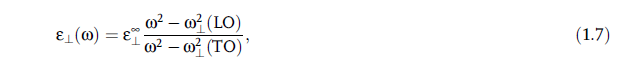
where and // indicate in the basal plane and along the c-direction, respectively.
Table 1.12 Parameters related to electrical and optical properties
of zinc blende GaN (in part after Refs [36,44]).

The details of the energies of high symmetry points are given in Table 2.1

which will be used to determine the optical frequency dielectric constant from the
knowledge of A1(LO) and A1(TO) phonon frequencies along the c-direction and
E1(LO) and E1(TO) in the basal plane. This relationship is used very often.
Parameters related to the energy bandgap, carrier mass, and mechanical properties
of AlN have been determined [71–76]. Extensive data on all the binary and ternary
band structure parameters can be found in Chapter 2. For example, additional
parameters on the critical point energies for Wz GaN, AlN, and InN are given in
Tables 2.1–2.3, respectively. Tables 2.4–2.6 list the critical point energies for ZB GaN,
AlN, and InN, respectively. Effective masses and other band parameters for Wz GaN
are listed in Table 2.9. Table 2.10 tabulates the Luttinger band parameters for ZBGaN.
Table 2.14 lists the effective band parameters for Wz AlN, whereas the effective
masses and band parameters for Wz AlN are tabulated in Table 2.15. Luttinger
parameters for ZB AlN are listed in Table 2.16. The band parameters and effective
masses for Wz InN are tabulated in Tables 2.19 and 1.20, respectively.
Returning to the content of this chapter, parameters associated with the mechanical
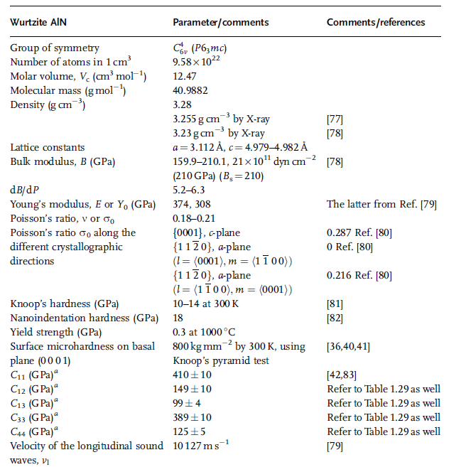
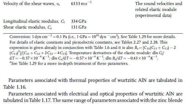
properties of AlN in wurtzitic and zinc blende phases are tabulated in Tables 1.13
and 1.14, respectively. The parameters related to the sound wave velocity in wurtzitic
AlN are listed in Table 1.15.
Table 1.13 Parameters related to mechanical properties of wurtzitic AlN (in part after Ref. [36]).
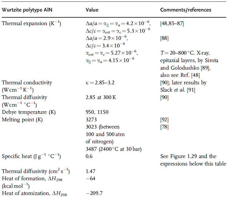
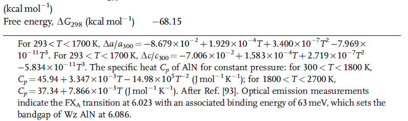
Parameters associated with thermal properties of wurtzitic AlN are tabulated in
Table 1.16.
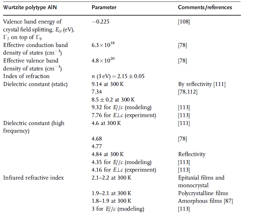
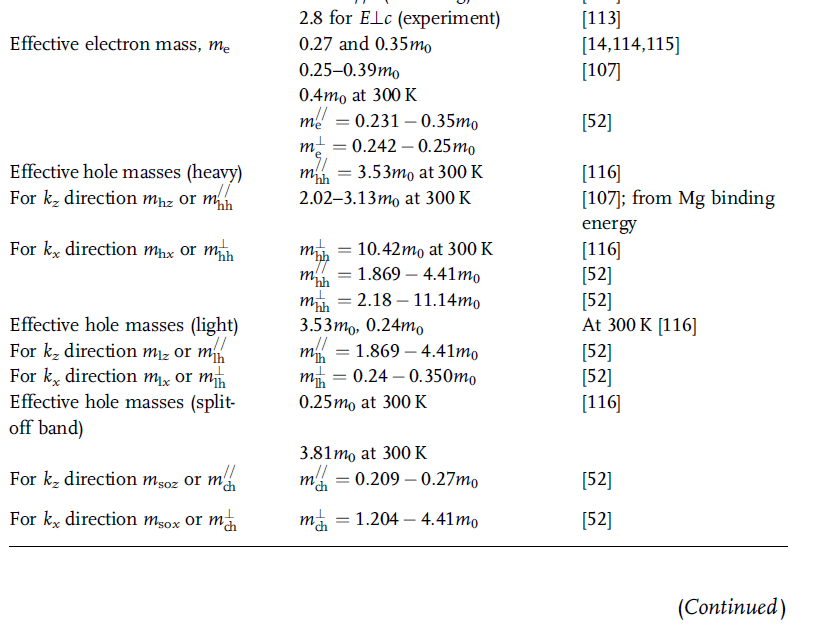
Parameters associated with electrical and optical properties of wurtzitic AlN are
tabulated in Table 1.17. The same range of parameters associated with the zinc blende
Table 1.14 Parameters related to mechanical properties of zinc blende AlN.

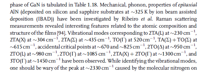
Table 1.15 Acoustic wave propagation properties in wurtzite AlN [36].
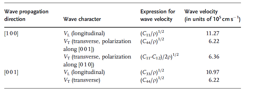
For the crystallographic directions, see Ref. [44].
the surface of c-Si [95]. It is worth noting that, owing to the extremely weak Raman
signal usually presented by AlN films, it is not uncommon to ascribe some of the
features erroneously to AlN [96].
Conduction band first- and second-order pressure derivatives [36]:
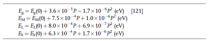
where P is pressure in kbar.
Table 1.17 Parameters related to optical and electrical properties
of wurtzitic AlN [97–102] (in part from Ref. [36]).
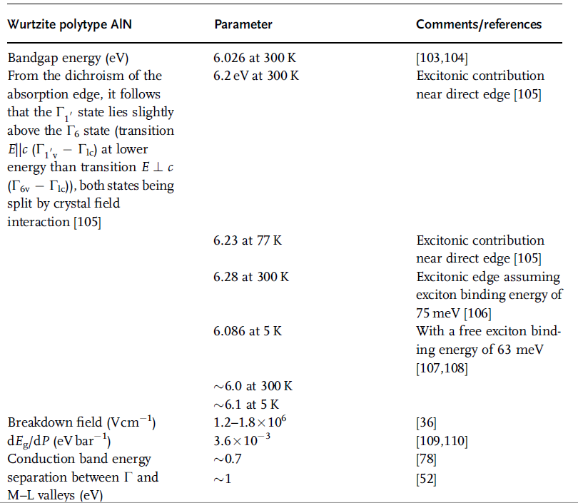

Table 1.17 (Continued)

Phase transition from the wurtzite phase to the rock salt structure (space
group O5
h; lattice parameter 4.04 Å) takes place at the pressure of 17 GPa (173 kbar)
[109,110].
Parameters associated with the electrical and optical properties of zinc blende AlN
are listed in Table 1.18. For details regarding the Luttinger parameters for the valence
band in zinc blende AlN, refer to Table 2.16. Parameters associated with the
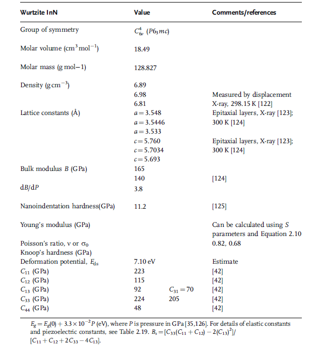
mechanical properties of wurtzitic InN are tabulated in Table 1.19.
For wurtzite crystal structure, the surfaces of equal energy in G valley should be
ellipsoids, but effective masses in the z-direction and perpendicular directions are
estimated to be approximately the same.
Table 1.18 Parameters related to optical and electrical properties of zinc blende AlN.
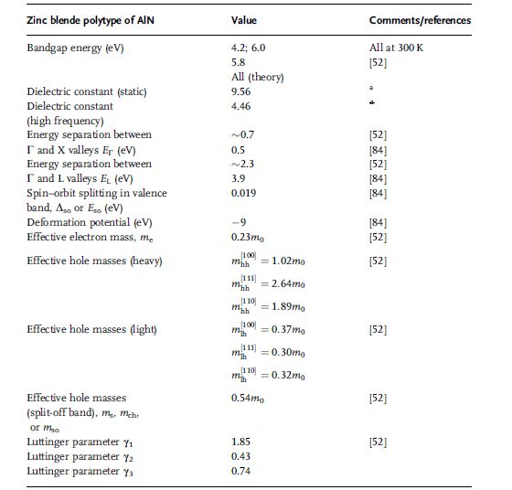
a C. Persson, and A. Ferreira da Silva, “Linear optical response of zinc-blende and wurtztie III-N
(III ¼ B, AI, Ga, and In)”, Journal of Crystal Growth 305 pp. 408–413 (2007)
The parameters associated with thermal properties of wurtzitic InN are tabulated
in Table 1.20.
The specific heat Cp of InN at constant pressure for 298 K<T<1273 K [51] is
Cp¼38.1þ1.21 · 102T (J mol1 K1). Refer to Table 1.31 for a detailed treatment of
mechanical properties of InN.
The parameters associated with electrical and optical properties of wurtzitic InN
are tabulated in Table 1.21.
Available parameters associated with the mechanical properties of zinc blende
InN, primarily calculated, are tabulated in Table 1.22. Other parameters dealing with
electrical and optical properties of zinc blende InN, primarily calculated, are listed in
Table 1.23.
Table 1.19 Parameters related to mechanical properties of wurtzitic InN (in part after Ref. [36]).