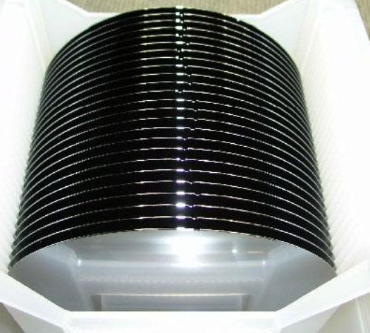
N-type or P-type 125mm silicon wafer can be supplied with the orientation of <111> or <100>. More specs are shown as following:
1. 125mm Silicon Substrate Wafer List
No. 1
| ID | 直径 | タイプ | ドーパント | オリ | RES (Ohm-cm) |
厚い(ええと) | ポーランド語 | グレード | 説明 |
| PAM2683 | 125mm | N | として | <111> | <0.0035 | 375um | SSP | メカ | メカニカルグレード。 EPIレイヤー:N / Phos Res:4.59-5.874ohm.cm 12-16um |
| PAM2684 | 125mm | N | P | <100> | <0.001 | 3000um | SSP | テスト | 厚さ3mm |
| PAM2685 | 125mm | P | B | <111> | 43485 | 525-575um | SSP | テスト | 現状有姿で販売 |
| PAM2686 | 125mm | P | B | <111> | 43485 | 500-550um | SSP | テスト | 現状有姿で販売 |
No. 2
| アイテム | 材料 | オリエント。 | ディアム (MM) |
Thck (μm) |
サーフ。 | 抵抗率 (Ωcm) |
コメント |
| PAM2687 | p型Si:B | [100] | 5 " | 889±13 | P / E | FZ> 1,000 | SEMI Prime、1Flat、Empak cst |
| PAM2688 | p型Si:B | [100] | 5 " | 920±10 | E / E | FZ> 1,000 | Empak cst |
| PAM2689 | p型Si:B | [100] | 5 " | 920±10 | E / E | FZ> 1,000 | 反り測定値<8μm、Empak cst |
| PAM2690 | N型Si:P | [100] | 5 " | 400 | P / E | FZ 7,000〜14,300 | SEMI Prime、1Flat、Empak cst、Bow / Warp <20μm |
| PAM2691 | N型Si:P | [100] | 5 " | 400 | P / E | FZ 7,000〜14,300 | SEMI Prime、1Flat、Bow / Warp <20μm |
| PAM2692 | N型Si:P | [100] | 5 " | 350 | P / E | FZ 5,000〜10,000 | SEMI Prime、1Flat、Empak cst、Bow / Warp <20μm |
| PAM2693 | N型Si:P | [100] | 5 " | 350 | P / E | FZ 5,000〜10,000 | SEMI Prime、1Flat、Bow / Warp <20μm、5枚のウェーハのEmpakカセット |
| PAM2694 | N型Si:P | [111]±0.1° | 5 " | 200±15 | 壊れた | FZ> 3,000 | 壊れたL / Lウェーハ、2枚 |
| PAM2695 | N型Si:P | [111] | 5 " | 300±15 | P / E | FZ 1,000〜3,000 | SEMI Prime、8枚のウェーハのハードカセット |
| PAM2696 | p型Si:B | [100] | 5 " | 625±15 | P / P | 16〜24 | SEMI Prime、Empak cst |
| PAM2697 | p型Si:B | [100] | 5 " | 600±10 | E / E | 2.0〜3.5 | SEMI、1フラット、コインロール |
| PAM2698 | p型Si:B | [100] | 5 " | 228 | P / P | 1〜10 | SEMI Prime、1Flat、Empak cst、TTV <5μm |
| PAM2699 | p型Si:B | [100] | 5 " | 525 | P / E | 1〜100 | シリコンリング。 4インチのウェーハを保持するための5インチの外径と4インチの内径 |
| PAM2700 | p型Si:B | [100] | 5 " | 625±15 | P / P | 1〜100 | SEMI Prime、Empak cst |
| PAM2701 | p型Si:B | [100] | 5 " | 990±8 | P / P | 1〜25 | SEMI Prime、Empak cst、TTV <1μm |
| PAM2702 | p型Si:B | [100] | 5 " | 525 | P / EOx | 0.002〜0.004 {0.0031〜0.0035} | SEMI Prime、1Flat、Striations–Free、TTV <5μm、裏面LTOシール厚さ0.50±0.05μm、各7枚のEmpakカセット |
| PAM2703 | p型Si:B | [100] | 5 " | 710 | E / E | RTP、1つのSEMIフラット、Open Empak cst | |
| PAM2704 | n型Si:As | [100] | 5 " | 625 | P / E | 0.001〜0.007 | セミテスト、2フラット、エンパックcst |
| PAM2705 | n型Si:As | [100] | 5 " | 625 | P / E | 0.001〜0.007 | セミテスト、2フラット、エンパックcst |
| PAM2706 | n型Si:Sb | [100]±1° | 5 " | 1,200±10 | P / E | 0.001〜0.025 | SEMIプライム、SEMIノッチ、TTV <1μmEmpakcst |
| PAM2707 | n型Si:As | [100] | 5 " | E / E | SEMI、1Flat、開いたEmpakcst | ||
| PAM2708 | n型Si:Sb | [100] | 5 " | E / E | SEMI 2Flats(2nd @ 135°)、開いたEmpakcst | ||
| PAM2709 | n型Si:Sb | [111–3.0°]±0.5° | 5 " | 625 | P / E | 0.015〜0.020 {0.0152〜0.0185} | SEMI Prime、2Flats、Empak cst |
| PAM2710 | 無作為に | 5 " | 無作為に | P / E | 無作為に | SEMIテスト、1Flat、Empak cst | |
| PAM2711 | 無作為に | 5 " | 無作為に | P / E | 無作為に | セミテスト、1フラット、エンパックcst | |
| PAM2712 | n型 | [100] | 5 " | 無作為に | P / EOx | 無作為に | セミテスト、2フラット(SF @ 180°)、裏面LTOシール、Empak cst |
| PAM2713 | [100] | 5 " | 無作為に | P / E | 無作為に | SEMIテスト、1Flat、Empak cst | |
| PAM2714 | n型 | [100] | 5 " | 無作為に | P / E | 無作為に | SEMIテスト、2フラット(2番目@ 180°)、Empak cst |
| PAM2715 | n型Si:As | [100] | 5 " | 625 | OxP / EOx | 0.001〜0.007 | SEMI Prime、2Flats、熱酸化3.5±0.5µm厚、Empak cst |
2. 125mm Silicon Wafer Industry Applicable Norms
2.1 Dimensions and Allowable Deviations of 125mm Silicon Substrate
If the size and its upper and lower limits of 5 inch silicon wafer are not specified in the detailed specification, the requirements shall be as follows:
| Size | Minimum | Target value | Standard Maximum | Maximum Epitaxial Layer |
| Diameter(mm) | 124.7 | 125 | 125.3 | 125.3 |
| Thickness at the Center(um) | 505 | 525 | 545 | 545 |
| Curvature(um) | – | – | 30 | 45 |
| Total Thickness Variation(um) | – | – | 5 | 9 |
| Flatness(um) | – | – | 3 | 5.5 |
| Warp(um) | – | – | 30 | 45 |
| Chipping(um) | – | – | 208 | – |
The flatness variation from the highest point to the lowest point of the ultra-flat test grade on the stepper used to test the focus cannot exceed 2 microns.
2.2 Silicon Wafer Crystal Orientation and Reference Plane Position
The crystal orientation of the 5” Si wafer surface should be indicated in the detailed specification. The allowable tolerance is 0.4 degrees. Orthogonal crystal orientation error shall not exceed 0.2 degrees;
Primary reference plane positioning: [110], no secondary reference plane within 1 degree;
Reference surface length: Main reference surface should be 42.5mm±2.5mm.
2.3 Doping Material of 125mm Silicon Thin Film
To obtain the P-type silicon wafer, Boron should be doped during the silicon wafer manufacturing process; and for the N-type 125mm wafer of silicon, Phosphorus should be doped.
2.4 Non-uniformity of 5” Si Substrate Radial Resistivity
| アイテム | <15 ohm-cm | >15 ohm-cm | ||
| N | P | N | P | |
| Center and 1/2 radius (R/2) | 9% | 4% | 11% | 6% |
| Center and 6 mm from the edge | 14% | 8% | 16% | 12% |
2.5 Other Requirements for 125mm Silicon Wafer:
One side of the 5 inch silicon substrate should be polished;
Silicon wafer growth method: Czochralski method;
125mm single crystal silicon wafer dislocation density: none;
Laser marking: It is required to meet the requirements of SEMI standard M1.1-85;
125mm silicon wafer defects limitation range: the area beyond 0.062 inches (1.57mm) from the edge of the silicon wafer is not included.
Note: Unless otherwise specified in the detailed specification, the silicon wafer manufacturing companies should use above requirements.
In order to ensure the production and delivery of fully qualified products, 125mm silicon wafers should be produced under an effective quality control system, including necessary staff training, procedures, equipment calibration, measurement and inspection. As part of quality control, key parameters should be tested regularly.

詳細については、メールでお問い合わせください。victorchan@powerwaywafer.com と powerwaymaterial@gmail.com.