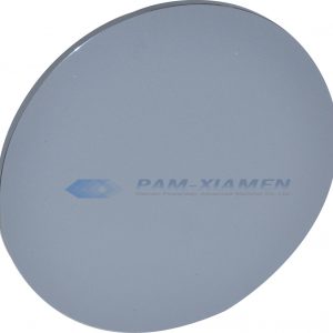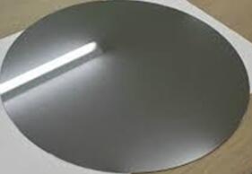
12インチプライムグレードシリコンウェーハ
PAM-XIAMEN offer 300mm bare silicon wafers (12 inch) in prime grade, n type or p type, and the 300mm silicon wafer thickness is 775±15. Compared to other silicon wafer suppliers, Powerway Wafer’s silicon wafer price is more competitive with higher quality. 300mm silicon wafers have a higher yield per wafer than pervious large diameter silicon wafers.
- 説明
製品の説明
PAM-XIAMEN offer 300mm bare silicon wafers (12 inch) in prime grade, n type or p type, and the 300mm silicon wafer thickness is 775±15. Compared to other silicon wafer suppliers, Powerway Wafer’s silicon device wafer price is more competitive with higher quality. 300mm silicon wafers have a higher yield per wafer than pervious large diameter silicon wafers. Size on/above 8 inches (200 mm) is called a large silicon wafer. The production technology of large silicon wafer is not only the increase of process complexity because of the increase of area, but also the higher requirements on many other control factors. For example: oxygen content and its radial uniformity in wafer, impurity control, OISF control, etc. The silicon wafer requirements for defect control, oxygen precipitation control, resistance quantification, doping and radial uniformity are also higher. Especially for prime grade 300mm silicon wafer, some parameters are required critically, for instant, wafer TTV is below1.5um and defect density ~0/cm2. The next step is 450mm silicon ingot or wafer.
1. Parameters of 300mm Silicon Wafer
| パラメータ | Value(PAM210512-300-SIL) |
| インゴットの種類 | チョクラルスキー法に従って成長 |
| 直径、mm | 300±0,2 |
| ドーパント | B(ボロン) |
| 導電型 | P |
| Oxigen max、OLD-PPMA | 40 |
| カーボン、PPMA | 1 |
| 結晶方位 | <100> |
| 結晶面の所定の面方位からの偏差、度 | 1 |
| 体積抵抗率、オーム・cm | 8-12 |
| 一次ノッチ | はい |
| ノッチ位置 | 110 |
| ノッチサイズ、mm | 2,3 |
| ノッチフォーム | V |
| ウェーハ厚、ミクロン | 775±15 |
| マーキングの種類 | レーザ |
| マーキング場所 | 裏側 |
| エッジプロファイル | SEMI T / 4より |
| 表面の傷 | ありません |
| 前面研磨 | はい |
| 裏面研磨 | はい |
| ウェーハの厚さの総変化(TTV)、マイクロ | 1,5 |
| たわみ(WARP)、ミクロン | 30 |
| 0.05ミクロンより大きい表面上の粒子の数 | 50 |
| 0.09ミクロンより大きい表面上の粒子の数 | 30 |
| アルミニウムの表面含有量、E10AT / CM2 | 1 |
| カルシウムの表面含有量、E10AT / CM2 | 1 |
| クロムの表面含有量、E10AT / CM2 | 1 |
| 銅の表面含有量、E10AT / CM2 | 1 |
| 鉄の表面含有量、E10AT / CM2 | 1 |
| カリウムの表面含有量、E10AT / CM2 | 1 |
| ナトリウムの表面含有量、E10AT / CM2 | 1 |
| ニッケルの表面含有量、E10AT / CM2 | 1 |
| 亜鉛の表面含有量、E10AT / CM2 | 1 |
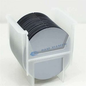
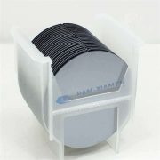
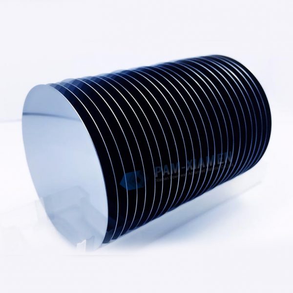
梱包要件:
| パラメータ | |
| 包装の種類 | MW300GT-A |
| 内容器素材 | ポリエチレン |
| 外装材 | アルミニウム |
| 1パッケージの個数 | 25 |
| 再利用性 | はい |
2. FAQ:
Q: Please take note that we offer “The number of particles on a surface larger than 0.09 microns 50” just for silicon substrate.
通常、粒子要件はシリコン基板です。
コンプライアンスを確保するために、確認していただけますか?
A: 再確認:はい、表示された情報は正しいです。
PAM-XIAMENは、テクノロジーとウェーハサポートを提供します。
詳細については、当社のウェブサイトをご覧ください。https://www.powerwaywafer.com/silicon-wafer,
で、私達に電子メールを送りますsales@powerwaywafer.comとpowerwaymaterial@gmail.com
関連製品
-
12 "のシリコンウェーハ300ミリメートルTOX(Siの熱酸化ウエハ)
PAM-XIAMEN offers 300mm silicon oxide wafer and dioxide wafer. Thermal oxide silicon wafer or silicon dioxide wafer is a bare silicon wafer with oxide layer grown by dry or wet oxidation process. The thermal oxide layer of the silicon wafer is usually grown in a horizontal tube furnace, and the silicon wafer oxide temperature range is generally 900 ℃ ~ 1200 ℃. Compared with CVD oxide layer, silicon wafer oxide layer has higher uniformity, better compactness, higher dielectric strength and better quality.
-
フロートゾーン単結晶シリコン
PAM-XIAMENでは、フロートゾーン法により得られるフロートゾーンシリコンウェーハを提供できます。 単結晶シリコンロッドはフロートゾーン成長によって得られ、その後、単結晶シリコンロッドをフロートゾーンシリコンウェーハと呼ばれるシリコンウェーハに加工します。 フローティングゾーンシリコンプロセス中、ゾーンメルトシリコンウェーハは石英るつぼと接触していないため、シリコン材料は浮遊状態にあります。 これにより、シリコンのフローティングゾーン溶解プロセス中の汚染が少なくなります。 炭素含有量と酸素含有量が低く、不純物が少なく、抵抗率が高くなります。 パワーデバイスや特定の高電圧電子デバイスの製造に適しています。
-
12「テストグレードシリコンウエハ
PAM-XIAMEN offers 300mm bare silicon wafers (12 inch) dummy, test grade, n type or p type. Compared to other silicon wafer suppliers, Powerway Wafer offers professional service with competitive prices.
-
CZ単結晶シリコン
PAM-XIAMEN, a monocrystalline bulk silicon producer, can offer <100>, <110> and <111> monocrystalline silicon wafers with N&P dopant in 76.2~200 mm, which are grown by CZ method. The Czochralski method is a crystal growth method, referred to as the CZ method. It is integrated in a straight-tube heat system, heated by graphite resistance, melts the polysilicon contained in a high-purity quartz crucible, and then inserts the seed crystal into the surface of the melt for welding. After that, the rotating seed crystal is lowered and melted. The body is infiltrated and touched, gradually raised, and finished or pulled through the steps of necking, necking, shouldering, equal diameter control, and finishing.
-
エピタキシャルシリコンウェーハ
Silicon Epitaxial Wafer(Epi Wafer) is a layer of epitaxial silicon single crystal deposited onto a single crystal silicon wafer(note: it is available to grow a layer of poly crystalline Silicon layer on top of a highly doped Singly crystalline silicon wafer, but it needs buffer layer (such as oxide or poly-Si) in between the bulk Si substrate and the top epitaxial silicon layer. It also can be used for thin film transistor.
-
テストウェーハモニターウェーハダミーウェーハ
PAM-XIAMENはダミーウェーハメーカーとして、生産装置に使用され、生産工程初期の安全性向上や納期確認、工程形状の評価に使用されるシリコンダミーウェーハ/テストウェーハ/モニターウェーハを提供しています。 ダミーシリコンウェーハは実験やテストに使用されることが多いため、そのサイズと厚さが重要な要素となることが多い。 100mm、150mm、200mm、300mmのダミーウエハをご用意しております。
-
ポリッシュウェーハ
PAM-XIAMEN can offer polished wafer, n type or p type with orientation at <100>, <110> or <111>. FZ polished wafers, mainly for the production of silicon rectifier (SR), silicon controlled rectifier (SCR), Giant Transistor (GTR), thyristor (GRO)
-
エッチングウェハ
The etching silicon wafers offered by PAM-XIAMEN are N type or P type etching wafers, which have low roughness, low reflectivity and high reflectivity. The etching wafer has the characteristics of low roughness, good glossiness and relatively low cost, and directly substitutes the polished wafer or epitaxial wafer which has relatively high cost to produce the electronic elements in some fields, reducing the costs.