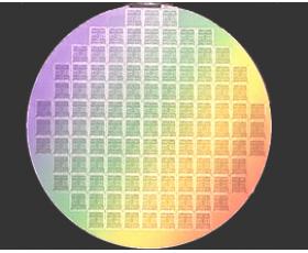
As one of leading SiC epi wafer suppliers, PAM-XIAMEN offers SiC epi wafer, and the SiC epi wafers type includes N type and P type. The SiC epi wafer thickness from 1um to 250um can be produced, and the silicon carbide epi wafer prices are competitive. What is SiC epi wafer? SiC epitaxial wafer is an intermediate link in the core of the SiC industry chain. At present, a whole set of industrial systems from silicon carbide substrates and SiC epi wafers to device preparation have been formed in the world. In the epi wafer market, high-quality SiC epitaxy are the basic materials of SiC power devices. The current development trend of silicon carbide epitaxial materials required by power electronic devices at home and abroad is developing in large diameter, low defects, high uniformity and etc.

1.4インチSiCエピウェーハの仕様
項目1:
PAM201221-SIC-EPI
| SiC基板 | |
| 直径 | 100ミリメートル |
| 厚さ | 350um |
| ポリタイプ | 4H-SiCの |
| 導電率 | N型 |
| オフの方向に向けて | 4度軸外 |
| MPD | ≤1/ cm2 |
| 抵抗率 | 0.015〜0.028オーム-cm |
| 表面仕上げ | 両面研磨 |
| エピ層 | |
| バッファ: | |
| 厚さ | 0.5um、n型 |
| ドーピングレベル | 1E18cm3 |
| エピ1: | |
| 厚さ | 6um +/- 5% |
| n-ドーピングレベル | 5.2E15 / cm3 |
項目2:
PAM210514-SIC-EPI
| SiC基板 | |
| 直径 | 100ミリメートル |
| 厚さ | 350um |
| ポリタイプ | 4H-SiCの |
| 導電率 | N型 |
| オフの方向に向けて | 4度軸外 |
| MPD | ≤1/ cm2 |
| 抵抗率 | 0.015〜0.028オーム-cm |
| 表面仕上げ | 両面研磨 |
| エピ層: | |
| バッファ: | |
| 厚さ | 0.5um、n型 |
| ドーピングレベル | 1E18cm3 |
| エピ1: | |
| 厚さ | 6um +/- 5% |
| n-ドーピングレベル | <1E15 / cm3 |
| 低O、B、PおよびAl元素: | B <0.06PPM; P <0.05PPM; Al <0.01PPM; Oなし |
2. SiC Epi in the Fields of Low Voltage, Medium Voltage and High voltage
用途としては、一般的に炭化ケイ素を低電圧、中電圧、高電圧の3つの領域に分けます。 低電圧の場合、それは主にPFCや電源などの一部の家電製品向けです。 中電圧は主に自動車用電子機器向けであり、中電圧は将来のSiCエピウェーハ開発の主な応用方向でもあります。 3つ目は、3300Vを超える鉄道輸送や電力網システムなど、比較的高い電圧レベルのアプリケーションエンドです。
同時に、中低電圧分野では炭化ケイ素と窒化ガリウムが依然として競争関係にあることがわかりますが、高電圧分野では、材料の成熟度の観点から、炭化ケイ素には独自の利点があります。 。 しかし、これまで高圧分野で成熟した製品がなかったのは残念です。 高電圧分野向けのSiCエピウェーハは世界中で研究開発の段階にありますが、中低電圧の炭化ケイ素エピタキシャルウェーハはすでに市場のダイオードやMOSFET製品に適用されています。
3. 100mm 4H SiC Epitaxial Wafer Norm
This norm applies to 4H silicon carbide (4H-SiC) epitaxial wafers. The SiC wafer production is mainly used to manufacture power semiconductor devices or power electronic devices.
3.1 Requirements of 4H-SiC Epitaxial Growth in 4 Inch
The substrate is a (0001) silicon surface 4H-SiC wafer with an angle of 4° in the <11-20> direction. The ratio of 4H crystal type to the total area of the silicon carbide wafer should not be less than 90%. The surface of the wafer can be polished on one side or on both sides. The silicon surface of the wafer should be chemically mechanically polished with a surface roughness of less than 0.5 nm. The number of cleanable particles on the surface of the wafer (diameter ≥0.5 um) does not exceed 15/piece.
3.2 Epitaxial Quality Requirements for the SiC wafer
Surface defects of SiC epitaxy should meet the requirements of the following table.
| Item | Maximum Allowable Limit | |
| Industrial Grade | Research Grade | |
| Carrots | ≤80pcs/wafer | ≤100pcs/wafer |
| Comets | ||
| Triangles | ||
| Downfalls | ||
| Edge Removal | 3 mm | 3 mm |
The surface roughness of SiC wafer in size of 4” should be less than 5.0 nm in the entire 4H-SiC epitaxial wafer range.
The thickness uniformity of the 4-inch SiC epitaxial layer should meet: industrial grade ≤5% and research grade ≤7%
Doping concentration uniformity for industrial grade should be ≤30%, and that for research grade should be ≤35%.
4. FAQ about SiC Epitaxy
Q1: I looked at the SiC homoepitaxial wafers on your company website before, and they all have buffer layer. I would like to ask what is the function of the intermediate buffer layer? What effect will it have on the epitaxial layer if directly epitaxial without a buffer layer?
A: The role of the intermediate buffer layer in SiC homoepitaxy is to reduce defect density and provide epitaxial yield.
Q2: Is there a big difference between the growth temperature of the buffer layer and the epitaxial layer of 4H-SiC epitaxial wafer?
A: There is little difference in growth temperature for buffer and epitaxial layer of 4H-SiC epi wafer.
Q3: I am interested in your standard Instrinsic SiC on 4H SiC substrate.The application is to produce electrochemically suspended membranes of ui doped SiC from a n-type substrate, hopefully of thicknesses between 500nm-2000nm. We are trying to determine the performance of our electrochemical undercut process on Si-face and C-face material. Does high wafer resistivity come from high compensation by deep levels, or from a low concentration of impurities in the epi-layer?
A: If so, I think you need 500nm undoped SiC on n-type SiC substrate. Suggest you use thicker thickness. If you must require 2um, we also can do it, the carrier concentration of undoped SiC should be <1E5, typical ~1E4.
Q4: Is it possible to have 4H-SiC epitaxial on 3C-SiC with 20-40micron thickness?
A: 4H-N SiC on 3C-N SiC is prone to phase transition and is not easy to control. Generally speaking, under epitaxial conditions, it is easier to form 3C crystal forms, so it is difficult to estimate the difficulty of epitaxial 4H on 3C. But we can supply 350um thick freestanding 3C-SiC substrate, more specifications please refer to https://www.powerwaywafer.com/3c-sic-wafer.html.
SiCエピウェーハの詳細については、以下を参照してください。
詳細については、メールでお問い合わせください。 victorchan@powerwaywafer.com と powerwaymaterial@gmail.com.

