1.Specs of AlGaInP Wafers on Chips
| パラメーター | 条件 | ミン。 | 標準。 | マックス。 | ユニット |
| 順方向電圧(Vf1) | If =10μA | 1.35 | ﹎ | ﹎ | V |
| 順方向電圧(Vf2) | If = 20mA | ﹎ | ﹎ | 2.2 | V |
| 逆電圧(Lr) | Vr = 10V | ﹎ | ﹎ | 2 | μA |
| 主波長(λd) | If = 20mA | 565 | ﹎ | 575 | NM |
| FWHM(Δλ) | If = 20mA | ﹎ | 10 | ﹎ | NM |
| コード | LC | LD | LE | LF | LG | LH | LI |
| IV(mcd) | 20-30 | 25-35 | 30-35 | 35-50 | 40-60 | 50-70 | 60-80 |
2. Band gap of strained AlGaInP on GaAs substrate
III-V化合物半導体とその合金のバンドパラメータ
I. Vurgaftman、JR Meyer、LR Ram-Mohan
J.Appl。 物理学89(11)、5815(2001)
| 1)AlP | 引張りひずみ | GaAsに関して |
| 2)GaP | 引張りひずみ | GaAsに関して |
| 3)InP | 圧縮的に歪む | GaAsに関して |
| 4)AlxGa1-xP | 引張りひずみ | GaAsに関して |
| 5)GaxIn1-xP | 緊張した | GaAsに関して |
| 6)AlxIn1-xP | 緊張した | GaAsに関して |
| 7)Al0.4Ga0.6P | 引張りひずみ | GaAsに関して |
| 8)Ga0.4In0.6P | 圧縮的に歪む | GaAsに関して |
| 9)Al0.4In0.6P | 圧縮的に歪む | GaAsに関して |
| シミュレーションでは、各材料層の長さは10nmです。 | ||
| 材料層4)、5)、および6)は、合金含有量を直線的に変化させます。 | ||
| 4)AlxGa1-xP(10 nm〜20 nm、x = 0.0〜x = 1.0) | ||
| 5)GaxIn1-xP(30 nm〜40 nm、x = 0.0〜x = 1.0) | ||
| 6)AlxIn1-xP(50 nm〜60 nm、x = 1.0〜x = 0.0) | ||
3. About AlGaInP/InGaP Structure
Since InGaAlP quaternary materials can have a wide direct band gap, by adjusting the composition of In, Al and Ga, they can be lattice-matched with high-quality and low-cost GaAs thin films. The light-emitting range of the epitaxial structure can cover red, orange, yellow, yellow-green band. Thus in the visible light emitting diode, 650nm red laser has a wide range of applications.
AlGaInP quaternary compound materials are used to grow GaAs epitaxial wafers, which are widely used in high-brightness red light emitting diodes and semiconductor lasers and have become the mainstream material for red light emitting devices. The conduction band order of AlGaInP/GaInP heterojunctions is very small, with a maximum value of about 270meV, which is smaller than that of 350meV AlGaAs materials. The electronic barrier is relatively low, and the leakage current is formed. The threshold current of the laser based GaAs epitaxy wafer is increased, which is more obvious in high temperature and high current operation. The AlGaInP layer will scatter in the alloy, and the thermal resistance is much higher than that of AlGaAs. The excess heat causes the junction temperature and cavity surface temperature. Therefore, the characteristic temperature of AlGaInP laser is lower, and the electro-optical conversion efficiency becomes lower during continuous operation, and more heat is generated.
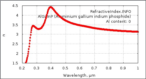
4. Refractive Index of AlGaInP
出典:PAM-厦門
詳細については、メールでお問い合わせください。victorchan@powerwaywafer.com と powerwaymaterial@gmail.com.