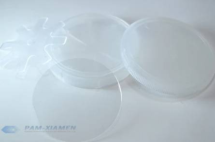
サファイアまたはシリコン基板上のAlScN(アルミニウムスカンジウムナイトライド)薄膜は、 PAM-厦門 SAW / FBARフィルター、オプトエレクトロニクスデバイス、パワーデバイス、MEMSのアプリケーション向け。 III-V半導体ベースの強誘電体であるAlScNは、現在有望な半導体材料であり、 AlN材料 5GRFフィールドで。 高含有量のスカンジウムを窒化アルミニウムにドープすることにより、高周波デバイスの圧電性能と電気機械結合係数を大幅に向上させることができます。 以下は、私たちからのAlScNテンプレートの基本情報です。
1.AlScNテンプレートの仕様
No.1サファイアベースのAlScNテンプレート
| パラメータ | C面サファイアウェーハ上のAlScNフィルム | ||
| Sl。 いいえ。 | PAM-050A | PAM-100A | PAM-150A |
| 直径 | 2” | 4インチ | 6インチ |
| Sc濃度 | 40±15% | ||
| AlScN膜厚 | 800 um | ||
| FWHM-HRXRD | ≤120秒角 | ||
| Ra [5x5um] | ≤10nm | ||
| TTV | ≤10um | ≤20um | ≤20um |
| 弓 | ≤20um | ≤40ええと | ≤60um |
| ワープ | ≤20um | ≤40ええと | ≤60um |
| サファイア基板 | |||
| 基板の厚さ | 430±15um | 650±20um | 1300±20um |
| 方向付け | c軸(0001)±0.2° | ||
| 使用可能エリア | > 95% | ||
| クラック | なし | ||
No.2SiベースのAlScNテンプレート
| パラメータ | C面シリコン基板上のAlScN膜 | ||
| Sl。 いいえ。 | PAM-100S | PAM-150S | PAM-200S |
| 直径 | 4インチ | 6インチ | 8インチ |
| Sc濃度 | 40±5% | ||
| AlScN膜厚 | 800 um | ||
| FWHM-HRXRD | ≤2° | ||
| Ra [5x5um] | ≤5nm | ||
| TTV | ≤10um | ≤5ええと | ≤4ええと |
| 弓 | ≤25um | ≤40ええと | ≤40ええと |
| ワープ | ≤25um | ≤40ええと | ≤40ええと |
| シリコン基板 | |||
| 基板の厚さ | 525±20um | 625±15um | 725±15um |
| 方向付け | c軸(0001)±0.2° | ||
| 導電率タイプ | N / P | ||
| 抵抗率 | > 5000オーム | ||
| 使用可能エリア | > 95% | ||
| クラック | なし | ||
2.高濃度にScをドープしたアルミニウムスカンジウムナイトライド膜の作製における困難と解決策
高濃度のScが組み込まれているため、三元窒化物合金の混合エントロピーは正であり、膜は準安定状態にあり、材料自体が相分解する傾向があります。 そのため、高Scドープ高品質AlScN膜の作製条件は非常に敏感であり、強誘電性アルミニウムスカンジウム窒化物薄膜の大量生産や下流の大規模産業用途を制限する大きな問題となっています。
Because Sc, Al, and N do not have solid solubility in thermal equilibrium, it is difficult to prepare Sc-Al or Sc-Al-N alloy targets. In the previous studies, most of the schemes used dual-target sputtering systems to prepare AlScN films. This scheme cannot prepare a thin film with uniform Sc concentration and uniform performance. With the increasing maturity of AlSc alloy target preparation technology, Sc-Al alloy ingots can basically meet the needs of various target materials. Therefore, the magnetron sputtering technology of alloy targets is used to prepare AlScN thin films. In 2010, Japan’s Akiyama et al used Sc0.42Al0.58 alloy targets to successfully fabricate Sc0.38Al0.62N films with a piezoelectric coefficient of 19 pC/N, which were combined with the Sc0.38Al0.62N films prepared by the double co-sputtering method. The piezoelectric constants are basically the same, which confirms the feasibility of AlSc alloy targets for preparing high-voltage electrical ScxAl1-xN films. At the same time, it is proposed that AlSc alloy targets are effective targets for keeping the concentration of scandium in ScxAl1-xN films constant. In 2017, Chiba University in Japan used an AlSc alloy target to grow a Sc0.32Al0.68N film, and successfully fabricated a SAW device with an electromechanical coupling coefficient greater than 2.5% based on the film material. In 2020, the University of Pennsylvania in the United States successfully fabricated a 1.5GHz SAW device with an electromechanical coupling coefficient as high as 4.78% based on the Si-based Al0.68Sc0.32N film.
スカンジウムをドープしたAlN薄膜中のScの濃度を上げると、材料の構造も純粋なウルツ鉱構造(AlN構造)から層状の六方晶構造(ScN準安定相)に移行します。 この変化は実験によって確認されています。 実際の操作では相転移の初期ドーピング濃度を決定することは困難であるため、合金材料中の遷移金属の溶解度を正確に決定することは困難です。 しかし、既存の文献は、AlNへの遷移金属の溶解度が低いことを示しています。 スカンジウムをドープしたAlN膜の相安定性と構造特性に関する研究では、スカンジウムをドープした濃度がx <56%の場合、六方晶のウルツ鉱構造が支配的であることが示されています。 スカンジウムをドープした濃度がx> 56%の場合、立方晶系が主な構造になります。

詳細については、メールでお問い合わせください。 victorchan@powerwaywafer.com と powerwaymaterial@gmail.com.