
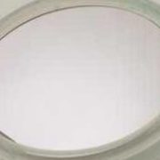


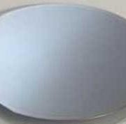

GaSbのウェハー
PAM-XIAMEN offers Compound Semiconductor GaSb wafer – gallium antimonide which are grown by LEC(Liquid Encapsulated Czochralski) as epi-ready or mechanical grade with n type, p type or semi-insulating in different orientation(111) or (100).
- 説明
製品の説明
PAM-XIAMEN offers Compound Semiconductor GaSb wafer – ガリウムアンチモン grown by LEC(Liquid Encapsulated Czochralski), which can reduce the defects of gallium antimonide. The GaSb wafer is epi-ready or mechanical grade with n type, p type or semi-insulating in different orientation(111) or (100).
Gallium antimonide (GaSb) is a semiconducting compound of gallium and antimony of the III-V family. It has a lattice constant of about 0.61 nm. GaSb wafers can be used for Infrared detectors,infrared LEDs and lasers and transistors, and thermophotovoltaic systems.
Here is the detail specification of wafer:
2 "(50.8ミリメートル)のGaSbウェーハ仕様
3 "(50.8ミリメートル)のGaSbウェーハの仕様
4」(100ミリメートル)のGaSbウェーハ仕様
2″ GaSb Wafer Specification
| tem | Specifications | ||
| Dopant | low doped | Zinc | Tellurium |
| Conduction Type | P-type | P-type | N-type |
| Wafer Diameter | 2″ | ||
| Wafer Orientation | (100)±0.5° | ||
| Wafer Thickness | 500±25um | ||
| Primary Flat Length | 16±2mm | ||
| Secondary Flat Length | 8±1mm | ||
| Carrier Concentration | (1-2)x1017cm-3 | (5-100)x1017cm-3 | (1-20)x1017cm-3 |
| Mobility | 600-700cm2/V.s | 200-500cm2/V.s | 2000-3500cm2/V.s |
| EPD | <2×103cm-2 | ||
| TTV | <10um | ||
| BOW | <10um | ||
| WARP | <12um | ||
| Laser Marking | upon request | ||
| Suface Finish | P/E, P/P | ||
| Epi Ready | yes | ||
| Package | Single wafer container or cassette | ||
3″ GaSb Wafer Specification
| tem | Specifications | ||
| Conduction Type | P-type | P-type | N-type |
| Dopant | low doped | Zinc | Tellurium |
| Wafer Diameter | 3″ | ||
| Wafer Orientation | (100)±0.5° | ||
| Wafer Thickness | 600±25um | ||
| Primary Flat Length | 22±2mm | ||
| Secondary Flat Length | 11±1mm | ||
| Carrier Concentration | (1-2)x1017cm-3 | (5-100)x1017cm-3 | (1-20)x1017cm-3 |
| Mobility | 600-700cm2/V.s | 200-500cm2/V.s | 2000-3500cm2/V.s |
| EPD | <2×103cm-2 | ||
| TTV | <12um | ||
| BOW | <12um | ||
| WARP | <15um | ||
| Laser marking | upon request | ||
| Suface finish | P/E, P/P | ||
| Epi ready | yes | ||
| Package | Single wafer container or cassette | ||
4″ GaSb Wafer Specification
| tem | Specifications | ||
| Dopant | low doped | Zinc | Tellurium |
| Conduction Type | P-type | P-type | N-type |
| Wafer Diameter | 4″ | ||
| Wafer Orientation | (100)±0.5° | ||
| Wafer Thickness | 800±25um | ||
| Primary Flat Length | 32.5±2.5mm | ||
| Secondary Flat Length | 18±1mm | ||
| Carrier Concentration | (1-2)x1017cm-3 | (5-100)x1017cm-3 | (1-20)x1017cm-3 |
| Mobility | 600-700cm2/V.s | 200-500cm2/V.s | 2000-3500cm2/V.s |
| EPD | <2×103cm-2 | ||
| TTV | <15um | ||
| BOW | <15um | ||
| WARP | <20um | ||
| Laser marking | upon request | ||
| Suface finish | P/E, P/P | ||
| Epi ready | yes | ||
| Package | Single wafer container or cassette | ||
1)2 "(50.8ミリメートル)、3"(76.2ミリメートル)のGaSbウェハ
Orientation:(100)±0.5°
Thickness(μm):500±25;600±25
Type/Dopant:P/low doped;P/Si;P/Zn
Nc(cm-3):(1~2)E17
Mobility(cm2/V ·s):600~700
Growth Method:CZ
Polish:SSP
2)2」(50.8ミリメートル)のGaSbウェハ
Orientation:(100)±0.5°
Thickness(μm):500±25;600±25
Type/Dopant:N/low doped;P/Te
Nc(cm-3):(1~5)E17
Mobility(cm2/V ·s):2500~3500
Growth Method:LEC
Polish:SSP
3)2」(50.8ミリメートル)のGaSbウェハ
Orientation:(111)A±0.5°
Thickness(μm):500±25
Type/Dopant:N/Te;P/Zn
Nc(cm-3):(1~5)E17
Mobility(cm2/V ·s):2500~3500;200~500
Growth Method:LEC
Polish:SSP
4)2」(50.8ミリメートル)のGaSbウェハ
Orientation:(111)B±0.5°
Thickness(μm):500±25;450±25
Type/Dopant:N/Te;P/Zn
Nc(cm-3):(1~5)E17
Mobility(cm2/V ·s):2500~3500;200~500
Growth Method:LEC
Polish:SSP
5)2」(50.8ミリメートル)のGaSbウェハ
Orientation:(111)B 2deg.off
Thickness(μm):500±25
Type/Dopant:N/Te;P/Zn
Nc(cm-3):(1~5)E17
Mobility(cm2/V ·s):2500~3500;200~500
Growth Method:LEC
Polish:SSP
相対製品:
InAsのウェハ
InSbのウェハ
InP基板
GaAs基板
GaSbのウェハ
GaPのウェーハ
ガリウムアンチモン(GaSbでは)のような切断、エッチング又は研磨仕上げを有するウェーハとして供給され、キャリア濃度、直径と厚さの広い範囲で利用可能であることができます。
GaSb material presents interesting gallium antimonide properties for single junction thermophotovoltaic (TPV) devices. GaSb: Te single crystal grown with Czochralski (Cz) or modified Czo- chralski (Mo-Cz) methods are presented and the problem of Te homogeneity discussed. As the carrier mobility is one of the key points for the gallium antimonide crystals, Hall measurements are carried out. We present here some complementary developments based on the material processing point of view: the bulk gallium antimonide crystal growth, the gallium antimonide wafer preparation, and the gallium antimonide wafer etching. Subsequent steps after these are related to the p / no r n/p junction elaboration. Some results obtained for different thin-layer elaboration approaches are presented. So from the simple vapor phase diffusion process or the liquid phase epitaxy process up to the metal organic chemical vapor deposition process, we report some material specificity.
We also offer gallium antimonide wafer epi service, take below as an example:
2”size GaSb epi wafer:
Epi layer: Thikness 0.5 um, undoped/p type GaSb epi layer (undoped InP epi layer also available),
Substrate:2” semi-insulating GaAs
Remark:
The Chinese government has announced new limits on the exportation of Gallium materials (such as GaAs, GaN, Ga2O3, GaP, InGaAs, and GaSb) and Germanium materials used to make semiconductor chips. Starting from August 1, 2023, exporting these materials is only allowed if we obtains a license from the Chinese Ministry of Commerce. Hope for your understanding and cooperation!
More epiwafer information, please read:
あなたも好きかも...
-
SiCウェーハ基板
The company has a complete SiC(silicon carbide) wafer substrate production line integrating crystal growth, crystal processing, wafer processing, polishing, cleaning and testing. Nowadays we supply commercial 4H and 6H SiC wafers with semi insulation and conductivity in on-axis or off-axis, available size:5x5mm2,10x10mm2, 2”,3”,4”, 6” and 8″, breaking through key technologies such as defect suppression, seed crystal processing and rapid growth, promoting basic research and development related to silicon carbide epitaxy, devices, etc.
-
InSbのウェハ
PAM-XIAMEN offers Compound Semiconductor InSb wafer – Indium antimonide wafer which is grown by LEC(Liquid Encapsulated Czochralski) as epi-ready or mechanical grade with n type, p type or semi-insulating in different orientation(111) or (100). Indium antimonide doped with isoelectronic(such as N doping) can reduce the defect density during the indium antimonide thin films manufacturing process.
-
GaAsのエピウェーハ
PAM-XIAMEN is manufacturing various types of epi wafer III-V silicon doped n-type semiconductor materials based on Ga, Al, In, As and P grown by MBE or MOCVD. We supply custom GaAs epiwafer structures to meet customer specifications, please contact us for more information.
-
ゲルマニウム(ゲルマニウム)単結晶とウェーハ
PAM-XIAMEN は、2 インチ、3 インチ、4 インチ、および 6 インチのゲルマニウム ウェーハを提供しています。これは、VGF / LEC によって成長させた Ge ウェーハの略です。 低濃度ドープの P 型および N 型ゲルマニウム ウェーハは、ホール効果の実験にも使用できます。 結晶ゲルマニウムは室温では脆く、可塑性がほとんどありません。 ゲルマニウムは半導体の性質を持っています。 高純度ゲルマニウムに三価元素(インジウム、ガリウム、ホウ素など)をドープすると、P 型ゲルマニウム半導体が得られます。 5価元素(アンチモン、ヒ素、リンなど)をドープしてN型ゲルマニウム半導体を得る。 ゲルマニウムは、高い電子移動度や高い正孔移動度など、優れた半導体特性を備えています。 -
GaP ウエハー – 一時的に提供できません
PAM-XIAMEN offers Compound Semiconductor GaP wafer – gallium phosphide wafer which is grown by LEC(Liquid Encapsulated Czochralski) as epi-ready or mechanical grade with n type, p type or semi-insulating in different orientation(111)or(100). -
InP基板
PAM-XIAMEN offers VGF InP(Indium Phosphide) wafer with prime or test grade including low dope, N type or semi-insulating. The mobility of InP wafer is different in different type, low doped one>=3000cm2/V.s, N type>1000 or 2000cm2V.s(depends on different doping concentration), P type: 60+/-10 or 80+/-10cm2/V.s(depends on different Zn doping concentration), and semi-insulting one>2000cm2/V.s, the EPD of Indium Phosphide is below 500/cm2 normally.
-
InAsのウェハ
PAM-XIAMEN offers Compound Semiconductor InAs wafer – indium arsenide wafer which are grown by LEC(Liquid Encapsulated Czochralski) as epi-ready or mechanical grade with n type, p type or semi-insulating in different orientation(111) or (100). In addition, InAs single crystal has high electron mobility and is an ideal material for making Hall devices.
-
自立GaN基板
PAM-アモイUHB-LEDおよびLDのためのものである(窒化ガリウム)GaN基板ウエハを、自立するための製造技術を確立しました。 ハイドライド気相エピタキシー(HVPE)技術によって成長させ、我々のGaN基板は、低欠陥密度を有します。


