


InAsのウェハ
PAM-XIAMEN は、化合物半導体 InAs ウェハ、つまり N 型、p 型、または異なる方向 (111) または (100) の半絶縁性を備えたエピレディまたはメカニカルグレードとして LEC (Liquid Encapsulated Czochralski) によって成長させたインジウムヒ素ウェハを提供しています。 さらに、InAs 単結晶は電子移動度が高く、ホール素子の作製に最適な材料です。
- 説明
製品の説明
PAM-XIAMEN は化合物半導体 InAs ウェーハを提供 –インジウムヒ素LEC(Liquid Encapsulated Czochralski)によってエピレディまたはメカニカルグレードとしてn型、p型、または半絶縁性の異なる方位(111)(100)または(110)で成長したウェーハ。 さらに、InAs 単結晶は電子移動度が高く、ホール素子の作製に最適な材料です。
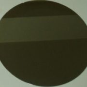
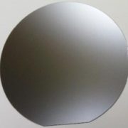
インジウムヒ素、InAs は、インジウムとヒ素から構成される半導体です。 融点 942 °C、格子定数 0.6058 nm の灰色の立方体結晶の外観を持ち、ヒ化インジダムの結晶構造は閃亜鉛鉱構造です。 インジウムヒ素ウェハは、1 ~ 3.8 µm の波長範囲の赤外線検出器の構築に使用されます。 検出器は通常、光起電力フォトダイオードです。 極低温冷却された検出器はノイズが低くなりますが、InAs 検出器は室温でも高出力アプリケーションに使用できます。 インジウムヒ素の優れた特性により、インジウムヒ素薄膜はダイオードレーザーの製造にも使用されます。
インジウムヒ素のバンドギャップはガリウムヒ素と同様の直接遷移であり、禁制帯幅は(300K)0.45eVです。 インジウムヒ素は、リン化インジウムと一緒に使用されることがあります。 ガリウムヒ素と合金化すると、In/Ga比に依存するバンドギャップを持つ材料であるインジウムガリウムヒ素が形成されます。これは主に窒化インジウムと窒化ガリウムを合金化して窒化インジウムガリウムを生成するのと同様の方法です。
ここでは詳細な仕様は次のとおりです。
2 "(50.8ミリメートル)のInAsウェーハ仕様
3 "(76.2ミリメートル)のInAsウェーハの仕様
4」(100ミリメートル)のInAsウェーハ仕様
2インチInAsウェーハ仕様
| アイテム | 仕様 | |||
| ドーパント | 低ドープ | スタナム | 硫黄 | 亜鉛 |
| 伝導型 | N型 | N型 | N型 | P型 |
| ウェーハ直径 | 2 " | |||
| ウェーハの向き | (111)±0.5°、(110)±0.5° | |||
| ウェーハの厚さ | 500±25um | |||
| 一次平坦長さ | 16±2mm | |||
| 二次平坦長さ | 8±1mm | |||
| キャリア濃度 | 5×1016cm-3 | (5-20)x1017cm-3 | (1-10)x1017cm-3 | (1-10)x1017cm-3 |
| モビリティ | ≧2×104cm2/Vs | 7000-20000cm2/Vs | 6000-20000cm2/Vs | 100-400cm2/Vs |
| EPD | <5×104cm-2 | <5×104cm-2 | <3×104cm-2 | <3×104cm-2 |
| TTV | <10um | |||
| 弓 | <10um | |||
| ワープ | <12um | |||
| レーザーマーキング | 要求に応じて | |||
| 表面仕上げ | P / E、P / P | |||
| エピ準備 | はい | |||
| パッケージ | 枚葉式ウェーハコンテナまたはカセット | |||
3インチInAsウェーハ仕様
| アイテム | 仕様 | |||
| ドーパント | 低ドープ | スタナム | 硫黄 | 亜鉛 |
| 伝導型 | N型 | N型 | N型 | P型 |
| ウェーハ直径 | 3 " | |||
| ウェーハの向き | (111)±0.5°、(110)±0.5° | |||
| ウェーハの厚さ | 600±25um | |||
| 一次平坦長さ | 22±2mm | |||
| 二次平坦長さ | 11±1mm | |||
| キャリア濃度 | 5×1016cm-3 | (5-20)x1017cm-3 | (1-10)x1017cm-3 | (1-10)x1017cm-3 |
| モビリティ | ≧2×104cm2/Vs | 7000-20000cm2/Vs | 6000-20000cm2/Vs | 100-400cm2/Vs |
| EPD | <5×104cm-2 | <5×104cm-2 | <3×104cm-2 | <3×104cm-2 |
| TTV | <12um | |||
| 弓 | <12um | |||
| ワープ | <15um | |||
| レーザーマーキング | 要求に応じて | |||
| 表面仕上げ | P / E、P / P | |||
| エピ準備 | はい | |||
| パッケージ | 枚葉式ウェーハコンテナまたはカセット | |||
4インチInAsウェーハ仕様
| アイテム | 仕様 | |||
| ドーパント | 低ドープ | スタナム | 硫黄 | 亜鉛 |
| 伝導型 | N型 | N型 | N型 | P型 |
| ウェーハ直径 | 4 " | |||
| ウェーハの向き | (111)±0.5°、(110)±0.5° | |||
| ウェーハの厚さ | 900±25um | |||
| 一次平坦長さ | 16±2mm | |||
| 二次平坦長さ | 8±1mm | |||
| キャリア濃度 | 5×1016cm-3 | (5-20)x1017cm-3 | (1-10)x1017cm-3 | (1-10)x1017cm-3 |
| モビリティ | ≧2×104cm2/Vs | 7000-20000cm2/Vs | 6000-20000cm2/Vs | 100-400cm2/Vs |
| EPD | <5×104cm-2 | <5×104cm-2 | <3×104cm-2 | <3×104cm-2 |
| TTV | <15um | |||
| 弓 | <15um | |||
| ワープ | <20um | |||
| レーザーマーキング | 要求に応じて | |||
| 表面仕上げ | P / E、P / P | |||
| エピ準備 | はい | |||
| パッケージ | 枚葉式ウェーハコンテナまたはカセット | |||
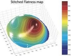
InAsウェーハのステッチ平坦度マップ
ウェハ仕様(例):
1)2” (50.8ミリメートル)のInAs
タイプ/ドーパント:N/S
方向:[111B]±0.5°
厚さ:500±25um
エピ対応
SSP
2)2” (50.8ミリメートル)のInAs
タイプ/ドーパント:N/低ドープ
方向: (111)B
厚さ:500um±25um
SSP
3)2” (50.8ミリメートル)のInAs
タイプ/ドーパント:N / 低ドープ
方位 : <111>A ±0.5°
厚さ:500um±25um
エピ対応
Ra<=0.5nm
キャリア濃度(cm-3):1E16~3E16
移動度(cm -2 ):>20000
EPD(cm -2 ):<15000
SSP
4)2” (50.8ミリメートル)のInAs
タイプ/ドーパント:N/低ドープ
方向: <100> と [001]OF
厚さ:2mm
ASカット
5)2” (50.8ミリメートル)のInAs
タイプ/ドーパント:N/P
方向:(100)、
キャリア濃度(cm-3):(5-10)E17、
厚さ:500μm
SSP
6)インジウムヒ素ウェーハ、
2”Ø×500±25μm、
p型InAs:Zn
(110)±0.5°、
Nc=(1-3)E18/cc 、
両面研磨、
枚葉カセットに窒素雰囲気下で密封されています。
すべてのウェーハは、高品質のエピタキシー準備仕上げで提供されています。 表面は、Surfscan(登録商標)ヘイズ及び粒子監視、分光エリプソメトリと斜入射干渉計を含む、社内、高度な光学計測技術によって特徴付けられます
ウェハのInAs、n型(1 0 0)における表面電子蓄積層の光学的性質にアニーリング温度の影響は、ラマン分光法によって研究されてきました。 それにより、非選別LOフォノンによる散乱のラマンピークはInAsの表面に電子蓄積層をアニールによって除去されていることを示す温度上昇と共に消失することを示します。 関与するメカニズムは、X線光電子分光法、X線回折および高分解能透過型電子顕微鏡により分析しました。 結果は、非晶質のIn 2 O 3及びAs 2 O 3相が焼鈍時のInAs表面に形成されていることを示しており、一方、酸化層とウエハとの間の界面における層のような薄い結晶は、表面電子の蓄積の厚さの減少につながるが生成されます吸着原子がアクセプタ型の表面状態を導入したよう以来の層。
InAsの発光波長は3.34μmであり、格子整合したIn-GaAsSb、InAsPSb、InAsSbマルチエピタキシャル材料をインジウム砒素基板上に成長させることができ、2~4μm帯の光ファイバー通信用のレーザーや検出器を製造できます。
当社では、InAs ウェーハ エピ サービスも提供しています。例として以下を取り上げます。
2インチサイズInAsエピウェハ(PAM190730-INAS):
エピ層:厚さ0.5μm、InAsエピ層(アンドープ、n型)、
基板:2 インチ半絶縁性 GaAs
InAs エピウェーハの詳細については、以下を参照してください。
あなたも好きかも...
-
InSbのウェハ
PAM-XIAMEN は、化合物半導体 InSb ウェハ – LEC (液体カプセル化チョクラルスキー) によって成長させた、n 型、p 型、または異なる方位 (111) または (100) の半絶縁性のエピレディまたはメカニカルグレードとして成長させたインジウムアンチモン化ウェハを提供しています。 等電子ドーピング(N ドーピングなど)されたインジウム アンチモン化物は、インジウム アンチモン化物薄膜製造プロセス中の欠陥密度を低減できます。
-
InP基板
PAM-XIAMEN は、低ドープ、N タイプ、または半絶縁性を含むプライムまたはテストグレードの VGF InP (リン化インジウム) ウェーハを提供しています。 InPウェハの移動度はタイプによって異なり、低ドープのもの>=3000cm2/Vs、Nタイプ>1000または2000cm2V.s(異なるドーピング濃度に依存)、Pタイプ:60+/-10または80+/-10cm2 /Vs(異なるZnドーピング濃度に依存)、半絶縁性のもの>2000cm2/Vs、リン化インジウムのEPDは通常500/cm2未満です。
-
GaSbのウェハー
PAM-XIAMEN は、LEC (Liquid Encapsulated Czochralski) によって成長された化合物半導体 GaSb ウェハ - アンチモン化ガリウムを、n 型、p 型、または異なる方位 (111) または (100) での半絶縁性のエピレディまたはメカニカルグレードとして提供しています。
-
GaP ウエハー – 一時的に提供できません
PAM-XIAMEN は、化合物半導体 GaP ウェーハ、つまり N 型、p 型、または異なる方位 (111) または (100) の半絶縁性を備えたエピレディまたはメカニカルグレードとして LEC (Liquid Encapsulated Czochralski) によって成長させたリン化ガリウムウェーハを提供しています。 -
GaN系HEMTエピタキシャルウェハ
窒化ガリウム (GaN) HEMT (高電子移動度トランジスタ) は、次世代の RF パワー トランジスタ技術です。 GaN テクノロジーのおかげで、PAM-XIAMEN は現在、サファイアまたはシリコン上の AlGaN/GaN HEMT エピ ウェーハと、サファイア テンプレート上の AlGaN/GaN を提供しています。
-
GaAsのエピウェーハ
PAM-XIAMEN は、MBE または MOCVD によって成長させた Ga、Al、In、As、P をベースとしたさまざまなタイプのエピ ウェハ III-V シリコンドープ n 型半導体材料を製造しています。 当社では、お客様の仕様を満たすカスタム GaAs エピウェーハ構造を提供しています。詳細については、お問い合わせください。
-
ゲルマニウム(ゲルマニウム)単結晶とウェーハ
PAM-XIAMEN は、2 インチ、3 インチ、4 インチ、および 6 インチのゲルマニウム ウェーハを提供しています。これは、VGF / LEC によって成長させた Ge ウェーハの略です。 低濃度ドープの P 型および N 型ゲルマニウム ウェーハは、ホール効果の実験にも使用できます。 結晶ゲルマニウムは室温では脆く、可塑性がほとんどありません。 ゲルマニウムは半導体の性質を持っています。 高純度ゲルマニウムに三価元素(インジウム、ガリウム、ホウ素など)をドープすると、P 型ゲルマニウム半導体が得られます。 5価の元素(アンチモン、ヒ素、リンなど)をドープすると、N型ゲルマニウム半導体が得られます。 ゲルマニウムは、高い電子移動度や高い正孔移動度など、優れた半導体特性を備えています。 -
SiCウェーハ基板
同社は、結晶成長、結晶処理、ウェーハ処理、研磨、洗浄、テストを統合した完全なSiC(炭化ケイ素)ウェーハ基板生産ラインを持っています。 現在、当社は、オンアクシスまたはオフアクシスで半絶縁性と導電性を備えた市販の 4H および 6H SiC ウェハーを供給しています。利用可能なサイズ: 5x5mm2、10x10mm2、2 インチ、3 インチ、4 インチ、6 インチ、および 8 インチ。欠陥抑制、種結晶加工、高速成長など、炭化珪素エピタキシー、デバイス等に関する基礎研究開発を推進します。