
InP基板
PAM-XIAMEN は、低ドープ、N タイプ、または半絶縁性を含むプライムまたはテストグレードの VGF InP (リン化インジウム) ウェーハを提供しています。 InPウェハの移動度はタイプによって異なり、低ドープのもの>=3000cm2/Vs、Nタイプ>1000または2000cm2V.s(異なるドーピング濃度に依存)、Pタイプ:60+/-10または80+/-10cm2 /Vs(異なるZnドーピング濃度に依存)、半絶縁性のもの>2000cm2/Vs、リン化インジウムのEPDは通常500/cm2未満です。
- 説明
製品の説明
InP基板
InP ウェーハの大手サプライヤーである PAM-XIAMEN は、化合物半導体 InP ウェーハを提供しています –Indium Phosphideこれらは、n型、p型、または半絶縁性のエピレディまたはメカニカルグレードとして、LEC(液体カプセル化チョクラルスキー)またはVGF(垂直勾配凍結)によって成長されます。 InPウェーハ方位(111)または(100)を選択可能です。 ドーパントは硫黄、スズ (スズ)、亜鉛、またはカスタムの場合があります。 プライマリ フラットとともに InP ウェハの裏面に指定どおりにレーザー マークを付けます。 [110]±0.025°に向かって(100)0.075°など、若干の偏角を持った配向も可能です。
リン化インジウム (InP) は、インジウムとリンで構成される二元半導体です。 これは、GaAs およびほとんどの III-V 族半導体と同一の面心立方晶 (「閃亜鉛鉱」) 結晶構造を持っています。 リン化インジウムは、白リンとヨウ化インジウムを400℃で反応させて製造することもできるし、精製した元素を高温高圧で直接組み合わせるか、トリアルキルインジウム化合物の混合物の熱分解によっても製造できる。そしてリン化物。 リン化インジウムウェーハは、より一般的な半導体であるシリコンやガリウムヒ素に比べて電子速度が優れているため、高出力および高周波エレクトロニクスで使用されています[要出典]。 弊社が提供できるInPウェーハサイズは2”、3”、4”で、InPウェーハの厚さは350~625umとなります。
ここでは詳細な仕様は次のとおりです。
| アイテム | 仕様 | |||
| ドーパント | N型 | N型 | P型 | SIタイプ |
| 伝導型 | 低ドープ | 硫黄 | 亜鉛 | lron |
| ウェーハ直径 | 2 " | |||
| ウェーハの向き | (100)が0.5°、±します | |||
| ウェーハの厚さ | 最小:325 最大:375 | |||
| 一次平坦長さ | 16±2mm | |||
| 二次平坦長さ | 8±1mm | |||
| キャリア濃度 | 3×1016cm-3 | (0.8-6)x1018cm-3 | (0.6-6)x1018cm-3 | N / A |
| モビリティ | (3.5-4)x103cm2/Vs | (1.5-3.5)x103cm2/Vs | 50~70×103cm2/Vs | >1000cm2/Vs |
| 抵抗率 | N / A | N / A | N / A | N / A |
| EPD | <1000cm-2 | <500cm-2 | <1×103cm-2 | <5×103cm-2 |
| TTV | <10um | |||
| 弓 | <10um | |||
| ワープ | <12um | |||
| レーザーマーキング | 要求に応じて | |||
| 表面仕上げ | P / E、P / P | |||
| エピ準備 | はい | |||
| パッケージ | 枚葉式ウェーハコンテナまたはカセット | |||
2インチPタイプInPウェハ仕様
| アイテム | パラメーター | 単位 |
| 材料 | InP | |
| 導電型/ドーパント | SCP/亜鉛 | |
| グレード | 素数 | |
| 直径: | 50.5±0.4 | ミリ |
| オリエンテーション: | (100)が0.5°、±します | |
| 方向角度: | / | |
| 厚さ: | 最小:325 最大:375 | ええと |
| キャリア濃度: | 最小:0.6E18 最大:3E18 | cm-3 |
| 抵抗率: | 最小:/ 最大:/ | ohm.cm |
| 可動性: | 最小:/ 最大:/ | cm-2/V.sec |
| EPD: | 平均<:1000 最大<:/ | cm-2 |
| TTV: | 最大:10 | ええと |
| TIR: | 最大:10 | ええと |
| 弓: | 最大:10 | ええと |
| ワープ: | 最大:15 | ええと |
| フラットオプション: | EJ | |
| プライマリフラット方向: | (0-1-1) | |
| 一次フラット長さ: | 16±1 | ミリ |
| 二次フラット方向: | (0-11) | |
| 二次平坦長さ: | 7±1 | ミリ |
| 表面: | 側面 1: 研磨 側面 2: エッチング | |
| エッジの丸み | 0.25(SEMI規格準拠) | mmR |
| 粒子数: | / | |
| パッケージ | N を充填した個別の容器2 | |
| エピレディ | はい | |
| レーザーマーキング | 裏側メジャーフラット | |
| リマーク: | 特殊仕様については別途ご相談させていただきます | |
3インチInPウェーハ仕様
| アイテム | 仕様 | |||
| ドーパント | N型 | N型 | P型 | SIタイプ |
| 伝導型 | 低ドープ | 硫黄 | 亜鉛 | lron |
| ウェーハ直径 | 3 " | |||
| ウェーハの向き | (100)が0.5°、±します | |||
| ウェーハの厚さ | 600±25um | |||
| 一次平坦長さ | 16±2mm | |||
| 二次平坦長さ | 8±1mm | |||
| キャリア濃度 | ≤3×1016cm-3 | (0.8-6)x1018cm-3 | (0.6-6)x1018cm-3 | N / A |
| モビリティ | (3.5-4)x103cm2/Vs | (1.5-3.5)x103cm2/Vs | 50~70×103cm2/Vs | >1000cm2/Vs |
| 抵抗率 | N / A | N / A | N / A | N / A |
| EPD | <1000cm-2 | <500cm-2 | <1×103cm-2 | <5×103cm-2 |
| TTV | <12um | |||
| 弓 | <12um | |||
| ワープ | <15um | |||
| レーザーマーキング | 要求に応じて | |||
| 表面仕上げ | P / E、P / P | |||
| エピ準備 | はい | |||
| パッケージ | 枚葉式ウェーハコンテナまたはカセット | |||
4インチInPウェーハ仕様
| アイテム | 仕様 | |||
| ドーパント | N型 | N型 | P型 | SIタイプ |
| 伝導型 | 低ドープ | 硫黄 | 亜鉛 | lron |
| ウェーハ直径 | 4 " | |||
| ウェーハの向き | (100)が0.5°、±します | |||
| ウェーハの厚さ | 600±25um | |||
| 一次平坦長さ | 16±2mm | |||
| 二次平坦長さ | 8±1mm | |||
| キャリア濃度 | ≤3×1016cm-3 | (0.8-6)x1018cm-3 | (0.6-6)x1018cm-3 | N / A |
| モビリティ | (3.5-4)x103cm2/Vs | (1.5-3.5)x103cm2/Vs | 50~70×103cm2/Vs | >1000cm2/Vs |
| 抵抗率 | N / A | N / A | N / A | N / A |
| EPD | <1000cm-2 | <500cm-2 | <1×103cm-2 | <5×103cm-2 |
| TTV | <15um | |||
| 弓 | <15um | |||
| ワープ | <15um | |||
| レーザーマーキング | 要求に応じて | |||
| 表面仕上げ | P / E、P / P | |||
| エピ準備 | はい | |||
| パッケージ | 枚葉式ウェーハコンテナまたはカセット | |||
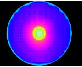
PL(フォトルミネッセンス)試験リン化インジウムウエハ
InP ウェーハを Peak Lambda、Peak int、FWHM によって測定します。スペクトル マッピングは次のとおりです。

InPウェーハアプリケーションについて
新しいタイプの化合物半導体材料として、InP ウェーハの市場シェアは徐々に増加しています。 リン化インジウムの優れた特性により、InP 材料で製造されたマイクロ波電源デバイス、マイクロ波増幅器、およびゲート FET の性能は、既存のガリウムヒ素材料で製造されたものよりも優れています。 リン化インジウムヘテロ接合レーザーも、光ファイバー通信において非常に有望な光源です。
ミリ波マイクロエレクトロニクスデバイスや光ファイバ通信用のオプトエレクトロニクスデバイス材料の成長など、デバイス用の InP ウェハ製造は広く使用されています。 デバイス性能の継続的な向上とデバイスサイズの縮小に伴い、リン化インジウムウェーハに対する品質要件はますます高くなっています。 したがって、InP ウェーハプロセスは徐々に最適化されています。
典型的な値は以下のデータを参照してください。
| ピークラムダ(nm) | ピーク内部 | 半値幅(nm) |
| 1279.4 | 7.799 | 48.5 |
| 1279.8 | 5.236 | 44.6 |
あなたも好きかも...
-
GaAs(ガリウム砒素)ウエハース
GaAs基板の大手サプライヤーとして、PAM-XIAMENはプライムグレードとダミーグレードの半導体n型、半導体Cドープ、p型を含むエピ対応GaAs(ガリウムヒ素)ウェハ基板を製造しています。 GaAs基板の抵抗率はドーパントに依存し、SiドープまたはZnドープのものは(0.001~0.009)Ω・cm、Cドープのものは>=1E7Ω・cmです。 GaAs ウェーハの結晶方位は (100) および (111) である必要があります。 (100) 方向の場合、2°/6°/15° ずらすことができます。 GaAs ウェーハの EPD は通常、LED の場合は <5000/cm2、LD またはマイクロエレクトロニクスの場合は <500/cm2 です。
-
InAsのウェハ
PAM-XIAMEN は、化合物半導体 InAs ウェハ、つまり N 型、p 型、または異なる方向 (111) または (100) の半絶縁性を備えたエピレディまたはメカニカルグレードとして LEC (Liquid Encapsulated Czochralski) によって成長させたインジウムヒ素ウェハを提供しています。 さらに、InAs 単結晶は電子移動度が高く、ホール素子の作製に最適な材料です。
-
GaP ウエハー – 一時的に提供できません
PAM-XIAMEN は、化合物半導体 GaP ウェーハ、つまり N 型、p 型、または異なる方位 (111) または (100) の半絶縁性を備えたエピレディまたはメカニカルグレードとして LEC (Liquid Encapsulated Czochralski) によって成長させたリン化ガリウムウェーハを提供しています。 -
InSbのウェハ
PAM-XIAMEN は、化合物半導体 InSb ウェハ – LEC (液体カプセル化チョクラルスキー) によって成長させた、n 型、p 型、または異なる方位 (111) または (100) の半絶縁性のエピレディまたはメカニカルグレードとして成長させたインジウムアンチモン化ウェハを提供しています。 等電子ドーピング(N ドーピングなど)されたインジウム アンチモン化物は、インジウム アンチモン化物薄膜製造プロセス中の欠陥密度を低減できます。
-
自立GaN基板
PAM-アモイUHB-LEDおよびLDのためのものである(窒化ガリウム)GaN基板ウエハを、自立するための製造技術を確立しました。 ハイドライド気相エピタキシー(HVPE)技術によって成長させ、我々のGaN基板は、低欠陥密度を有します。
-
SiCのエピタキシー
我々は、カスタム薄膜(シリコンカーバイド)、炭化ケイ素デバイスの開発のため6H又は4H基板上のSiCエピタキシーを提供します。 SiCエピタキシャルウェハは、主にショットキーダイオード、金属酸化膜半導体電界効果トランジスタ、接合型電界効果のために使用されます -
ゲルマニウム(ゲルマニウム)単結晶とウェーハ
PAM-XIAMEN は、2 インチ、3 インチ、4 インチ、および 6 インチのゲルマニウム ウェーハを提供しています。これは、VGF / LEC によって成長させた Ge ウェーハの略です。 低濃度ドープの P 型および N 型ゲルマニウム ウェーハは、ホール効果の実験にも使用できます。 結晶ゲルマニウムは室温では脆く、可塑性がほとんどありません。 ゲルマニウムは半導体の性質を持っています。 高純度ゲルマニウムに三価元素(インジウム、ガリウム、ホウ素など)をドープすると、P 型ゲルマニウム半導体が得られます。 5価の元素(アンチモン、ヒ素、リンなど)をドープすると、N型ゲルマニウム半導体が得られます。 ゲルマニウムは、高い電子移動度や高い正孔移動度など、優れた半導体特性を備えています。 -
GaSbのウェハー
PAM-XIAMEN は、LEC (Liquid Encapsulated Czochralski) によって成長された化合物半導体 GaSb ウェハ - アンチモン化ガリウムを、n 型、p 型、または異なる方位 (111) または (100) での半絶縁性のエピレディまたはメカニカルグレードとして提供しています。