Silicon carbide has very stable characteristics, so that it can work stably in some harsh environments. Because of the stable chemical bonds, the technical threshold for silicon carbide production is very high. The growth conditions of silicon carbide crystal ingots are harsh, requiring high temperature (~2600℃) and high [...]
2021-04-23メタ著者
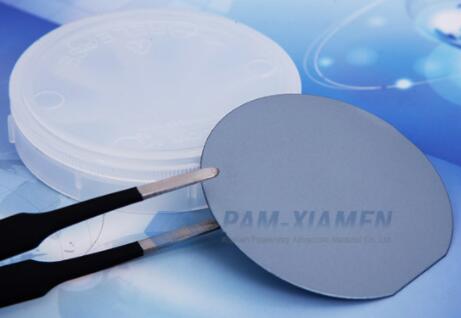
PAM XIAMEN offers 80+1mm FZ Si Ingot-2
FZ Si Ingot
Diameter 80+1mm, N-type, <111>±2°
Resistivity 1000-3000Ωcm
Oxygen/Carbon Content 10Е16см-3
The silicon content not less than 99.999999%
Length 150-480mm
MCC lifetime>1000μs
The dislocation density not, Swirl not
For more information, send us email at sales@powerwaywafer.com and powerwaymaterial@gmail.com
2020-03-18メタ著者
We are an expert of semiconductor wafers in semiconductor industry, and we offer technology support and wafers selling for thousands of univerisities and industrial customers by our decades experience, including Cornell University, Stanford Univeristy,Peking University, Shandong Univerity, university of south carolina,Caltech Faraon lab (USA),University of California, Irvine (USA),Singapore MIT Alliance for Research and Technology Centre (SMART),West Virginia University,Purdue Univerity, University of California, Los Angeles,King Abdullah University of Science & Technology,Massachusetts Institute of Technology,University of Houston,University of Wisconsin,University of Science and Technology of China etc.
And now we show one article example as follows, who bought our wafers or service:
Article title:Multisite microLED optrode array for neural interfacing
Published by:
Niall McAlinden; Yunzhou Cheng; Robert Scharf; Enyuan Xie; Erdan Gu; Christopher F. Reiche; [...]
2019-12-09メタ著者
PAM XIAMEN offers Si+SiO2 +Ti( or TiO2)+Pt Thin film.
Si+SiO2 +Ti( or TiO2)+Pt (111) Highly Oriented Polycrystal
SiO2+Ti+Pt (111) thin film on Si substrate, 5x5x0.525mm, 1sp, P-type, B-doped, (SiO2=300nm, Ti=10nm, Pt(111)=150nm)
SiO2+Ti+Pt(111) thin film on Si substrate ,10x10x0.525mm,1sp P-type B-doped,( SiO2=300nm,Ti=10nm ,Pt(111)=150nm)
SiO2+Ti+Pt(111) thin [...]
2019-05-16メタ著者
PAM XIAMEN offers YSGG single crystal.
PAM XIAMEN is developing a series of doped GGG single crystal for nest generation Magneto-optical device.
Composition
GGG
YSGG
S-GGG(CaMgZr:GGG)
NGG
GYSGG
GSGG
(Cubic)
Gd3Ga5O12
Y3Sc2Ga3O5
Gd2.6Ca0.4Ga4.1Mg0.25Zr0.65O12
Nd3Ga5O12
Gd0.63Y2.37Sc2Ga3O12
Gd3Sc2Ga3O12
Lattice constant
12.376 Å
12.426 Å ,
12.480 Å
12.505Å
12.507 Å ,
12.554 Å ,
Diffraction(2θ)
51º7′
50º44′
50º43′
50º41′
50º40′
50º22′
Melting Point
~1800 oC
~1877℃
~1730 oC
~1550 oC
~1730 oC
~1730 oC
For more information, please visit our website: https://www.powerwaywafer.com,
send us email at [...]
2019-05-21メタ著者
PAM XIAMEN offers 200mm Si wafers. Please send us email at sales@powerwaywafer.com if you need other specs and quantity.
Below are just some of our recent 200mm silicon wafer sale specials.
8″ silicon wafer
Dia.: 200+/-0.5mm
Type: P
Ori.: <100>
Res.: 1000-3000 ohm.cm
Thk.: 705-745um
V-notch
Surface: Polished/Etched
MFG: MEMC
200mm Silicon from PAM XIAMEN
200mm N/Ph [...]
2019-02-20メタ著者