
自立GaN基板
PAM-アモイUHB-LEDおよびLDのためのものである(窒化ガリウム)GaN基板ウエハを、自立するための製造技術を確立しました。 ハイドライド気相エピタキシー(HVPE)技術によって成長させ、我々のGaN基板は、低欠陥密度を有します。
- 説明
製品の説明
自立GaN基板
PAM-XIAMENはGaN基板のトップサプライヤーとして、自立型(窒化ガリウム)の製造技術を確立しました。GaN基板ウエハこれは、UHB-LED、LD、および MOS ベースのデバイスの製造用のバルク GaN 基板です。 水素化物気相エピタキシー (HVPE) 技術によって成長した当社のGaN基板III族窒化物デバイスの場合、欠陥密度が低く、マクロ欠陥密度が少ないかまったくありません。 GaN基板の厚さは330~530μmです。
GaN LED基板は電気特性が向上し、その性能が現在のデバイスを上回るため、パワーデバイスに加えて、窒化ガリウム半導体基板が白色光LEDの製造に使用されることが増えています。 さらに、窒化ガリウム基板技術の急速な発展により、欠陥密度が低く、マクロ欠陥密度が少ない高効率のGaN自立基板が開発されました。 したがって、このようなGaN基板は白色LEDにますます使用される可能性があります。 その結果、バルクGaN基板市場は急速に成長しています。 ちなみに、バルク GaN ウェーハは、垂直パワーデバイスのコンセプトをテストするために使用できます。
1. Specification of Freestanding GaN substrate
ここでは詳細な仕様を示しています。
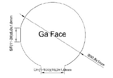
1.1 4″ N type Si doped GaN(Gallium Nitride) Free-standing Substrate
| アイテム | PAM-FS-GaN100-N+ |
| 伝導型 | N型/Siドープ |
| サイズ | 4インチ(100)+/-1mm |
| 厚さ | 480 +/- 50 |
| 方向付け | C軸(0001)+/- 0.5o |
| プライマリフラット場所 | (10-10)+/-0.5o |
| プライマリフラット長 | 32 +/- 1mm |
| セカンダリフラット場所 | (1-210)+/-3o |
| セカンダリフラット長 | 18+/-1mm |
| 抵抗率(300K) | <0.05Ω・cmで |
| 転位密度 | <5x106cm-2 |
| FWHM | <=100 秒角 |
| TTV | <= 30um |
| 弓 | <= +/- 30um |
| 表面仕上げ | 前面:Ra<=0.3nm。エピ対応研磨済み |
| — | 裏面:1.細かい研磨 |
| — | 2.研磨。 |
| 使用可能エリア | ≥ 90% |
1.2 4″ N Type Low Doped GaN(Gallium Nitride) Free-standing Substrate
| アイテム | PAM-FS-GaN100-N- |
| 伝導型 | N type |
| サイズ | 4インチ(100)+/-1mm |
| 厚さ | 480 +/- 50 |
| 方向付け | C軸(0001)+/- 0.5o |
| プライマリフラット場所 | (10-10)+/-0.5o |
| プライマリフラット長 | 32 +/- 1mm |
| セカンダリフラット場所 | (1-210)+/-3o |
| セカンダリフラット長 | 18+/-1mm |
| 抵抗率(300K) | <0.5Ω・cmで |
| 転位密度 | <5x106cm-2 |
| FWHM | <=100 秒角 |
| TTV | <= 30um |
| 弓 | <= +/- 30um |
| 表面仕上げ | 前面:Ra<=0.3nm。エピ対応研磨済み |
| — | 裏面:1.細かい研磨 |
| — | 2.研磨。 |
| 使用可能エリア | ≥ 90% |
1.3 4″ Semi-Insulating GaN(Gallium Nitride) Free-standing Substrate
| アイテム | PAM-FS-GaN100-SI |
| 伝導型 | 半絶縁 |
| サイズ | 4インチ(100)+/-1mm |
| 厚さ | 480 +/- 50 |
| 方向付け | C軸(0001)+/- 0.5o |
| プライマリフラット場所 | (10-10)+/-0.5o |
| プライマリフラット長 | 32 +/- 1mm |
| セカンダリフラット場所 | (1-210)+/-3o |
| セカンダリフラット長 | 18+/-1mm |
| 抵抗率(300K) | > 10 ^6Ω・cm |
| 転位密度 | <5x106cm-2 |
| FWHM | <=100 秒角 |
| TTV | <= 30um |
| 弓 | <= +/- 30um |
| 表面仕上げ | 前面:Ra<=0.3nm。エピ対応研磨済み |
| — | 裏面:1.細かい研磨 |
| — | 2.研磨。 |
| 使用可能エリア | ≥ 90% |
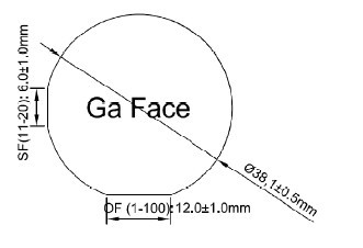
1.4 2″ Si doped GaN(Gallium Nitride) Free-standing Substrate
| アイテム | PAM-FS-GaN50-N+ | |||
| 伝導型 | N型/Siドープ | |||
| サイズ | 2」(50.8)+/- 1ミリメートル | |||
| 厚さ | 400 +/- 50 | |||
| 方向付け | C軸(0001)+/- 0.5o | |||
| プライマリフラット場所 | (10-10)+/-0.5o | |||
| プライマリフラット長 | 16 +/- 1ミリメートル | |||
| セカンダリフラット場所 | (1-210)+/-3o | |||
| セカンダリフラット長 | 8 +/- 1ミリメートル | |||
| 抵抗率(300K) | <0.05Ω・cmで | |||
| 転位密度 | <5x106cm-2 | |||
| FWHM | <=100 秒角 | |||
| TTV | <=15μmから | |||
| 弓 | <= +/- 20um | |||
| 表面仕上げ | 前面:Ra<=0.3nm。エピ対応研磨済み | |||
| 裏面:1.細かい研磨 | ||||
| 2.研磨。 | ||||
| 使用可能領域 | ≥ 90% | |||
1.5 2″ Low doped GaN(Gallium Nitride) Free-standing Substrate
| アイテム | PAM-FS-GaN50-N- | ||||
| 伝導型 | N type | ||||
| サイズ | 2」(50.8)+/- 1ミリメートル | ||||
| 厚さ | 400 +/- 50 | ||||
| 方向付け | C軸(0001)+/- 0.5o | ||||
| プライマリフラット場所 | (10-10)+/-0.5o | ||||
| プライマリフラット長 | 16 +/- 1ミリメートル | ||||
| セカンダリフラット場所 | (1-210)+/-3o | ||||
| セカンダリフラット長 | 8 +/- 1ミリメートル | ||||
| 抵抗率(300K) | <0.5Ω・cmで | ||||
| 転位密度 | <5x106cm-2 | ||||
| FWHM | <=100 秒角 | ||||
| TTV | <=15μmから | ||||
| 弓 | <= +/- 20um | ||||
| 表面仕上げ | 前面:Ra<=0.3nm。エピ対応研磨済み | ||||
| 裏面:1.細かい研磨 | |||||
| 2.研磨。 | |||||
| 使用可能領域 | ≥ 90% | ||||
1.6 2″ Semi-Insulating GaN(Gallium Nitride) Free-standing Substrate
| アイテム | PAM-FS-GaN50-SI | ||||
| 伝導型 | 半絶縁 | ||||
| サイズ | 2」(50.8)+/- 1ミリメートル | ||||
| 厚さ | 400 +/- 50 | ||||
| 方向付け | C軸(0001)+/- 0.5o | ||||
| プライマリフラット場所 | (10-10)+/-0.5o | ||||
| プライマリフラット長 | 16 +/- 1ミリメートル | ||||
| セカンダリフラット場所 | (1-210)+/-3o | ||||
| セカンダリフラット長 | 8 +/- 1ミリメートル | ||||
| 抵抗率(300K) | > 10 ^6Ω・cm | ||||
| 転位密度 | <5x106cm-2 | ||||
| FWHM | <=100 秒角 | ||||
| TTV | <=15μmから | ||||
| 弓 | <= +/- 20um | ||||
| 表面仕上げ | 前面:Ra<=0.3nm。エピ対応研磨済み | ||||
| 裏面:1.細かい研磨 | |||||
| 2.研磨。 | |||||
| 使用可能領域 | ≥ 90% | ||||
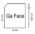
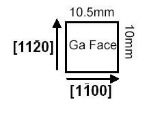
1.7 15mm,10mm,5mm フリースタンディングGaN系基板
| アイテム | PAM-FS-GaN15-N | PAM-FS-GaN15-SI | |
| PAM-FS-GaN10-N | PAM-FS-GaN10-SI | ||
| PAM-FS-GaN5-N | PAM-FS-GaN5-SI | ||
| 伝導型 | N型 | 半絶縁性 | |
| サイズ | 14.0mm*15mm 10.0mm*10.5mm 5.0*5.5mm | ||
| 厚さ | 330-450um | ||
| 方向付け | C軸(0001)+/- 0.5o | ||
| プライマリフラット場所 | |||
| プライマリフラット長 | |||
| セカンダリフラット場所 | |||
| セカンダリフラット長 | |||
| 抵抗率(300K) | <0.5Ω・cmで | >106Ω・cmで | |
| 転位密度 | <5x106cm-2 | ||
| マルコ欠陥密度 | 0cm-2 | ||
| TTV | <=15μmから | ||
| 弓 | <= 20umの | ||
| 表面仕上げ | 前面:磨かRA <0.2nm.Epi対応 | ||
| 裏面:1.Fineグラウンド | |||
| 2.Roughはすっ | |||
| 使用可能エリア | ≥90% | ||
注:
検証ウェーハ:使用の利便性を考慮して、PAM-XIAMEN は 2 インチ未満のサイズの自立型 GaN 基板用の 2 インチのサファイア検証ウェハを提供しています
2. Properties of Freestanding GaN Substrate
| Lattice Parameters | a=0.3189nm; c=0.5185nm |
| Band Gap | 3.39eV |
| Density | 6.15g/cm3 |
| Therm. Expansion Coefficient | a: 5.59×10⁻⁶/K; c: 3.17×10⁻⁶/K |
| Refraction Index | 2.33-2.7 |
| Dielectric Constant | 9.5 |
| Thermal Conductivity | 1.3W/(cm*k) |
| Break-Down Electrical Field | 3.3MV/cm |
| Saturation Drift Velocity | 2.5E7cm/s |
| Electron Mobility | 1300cm2/(V*s) |
3. Application of GaN Substrate
固体照明は:GaNデバイスは、超高輝度発光ダイオード(LED)、テレビ、自動車、一般照明として使用されます
DVD ストレージ: 青色レーザー ダイオード
パワーデバイス: GaNバルク基板上に製造されたデバイスは、携帯電話基地局、衛星、パワーアンプ、電気自動車(EV)やハイブリッド電気自動車(HEV)用のインバータ/コンバータなどの大電力および高周波パワーエレクトロニクスのさまざまなコンポーネントとして使用されます。 )。 GaN は (他の III 族窒化物と同様に) 電離放射線に対する感度が低いため、衛星用の太陽電池アレイや、通信、気象、監視衛星用の高出力高周波デバイスなどの宇宙搭載用途に適した材料となっています。
純粋な窒化ガリウム基板 IIII族窒化物の再成長に関する取引
ワイヤレス基地局:RFパワートランジスタ
ワイヤレスブロードバンドアクセス:高周波MMICの、RF-回路のMMICの
圧力センサー:MEMS
熱センサー:パイロ電気検出器
Powerコンディショニング:混合信号のGaN / Siの統合
カーエレクトロニクス:高温エレクトロニクス
送電線:高電圧エレクトロニクス
フレームセンサー:UV検出器
太陽電池: GaN の広いバンドギャップは、0.65 eV から 3.4 eV の太陽スペクトル (実質的に太陽スペクトル全体) をカバーし、窒化インジウム ガリウムを形成します。
太陽電池材料を作成するための完璧な(InGaN系)の合金。 このため有利で、GaN基板上に成長させたInGaN太陽電池は、GaN基板ウェーハのための最も重要な新しいアプリケーションや成長市場の一つになろうとしています。
HEMT、FETのための理想
GaN ショットキー ダイオード プロジェクト: HVPE で成長させた n 型および p 型の自立窒化ガリウム (GaN) 層上に製造されたショットキー ダイオードのカスタム仕様を受け入れます。
両方の接点 (オーム接点とショットキー接点) は、Al/Ti および Pd/Ti/Au を使用して上面に堆積されました。
述べる:
中国政府は、半導体チップの製造に使用されるガリウム材料(GaAs、GaN、Ga2O3、GaP、InGaAs、GaSbなど)およびゲルマニウム材料の輸出に対する新たな制限を発表しました。 2023 年 8 月 1 日より、これらの材料の輸出は中国商務省から許可を取得した場合にのみ許可されます。 ご理解とご協力をお願いいたします。
あなたも好きかも...
-
ゲルマニウム(ゲルマニウム)単結晶とウェーハ
PAM-XIAMEN は、2 インチ、3 インチ、4 インチ、および 6 インチのゲルマニウム ウェーハを提供しています。これは、VGF / LEC によって成長させた Ge ウェーハの略です。 低濃度ドープの P 型および N 型ゲルマニウム ウェーハは、ホール効果の実験にも使用できます。 結晶ゲルマニウムは室温では脆く、可塑性がほとんどありません。 ゲルマニウムは半導体の性質を持っています。 高純度ゲルマニウムに三価元素(インジウム、ガリウム、ホウ素など)をドープすると、P 型ゲルマニウム半導体が得られます。 5価の元素(アンチモン、ヒ素、リンなど)をドープすると、N型ゲルマニウム半導体が得られます。 ゲルマニウムは、高い電子移動度や高い正孔移動度など、優れた半導体特性を備えています。 -
InP基板
PAM-XIAMEN offers VGF InP(Indium Phosphide) wafer with prime or test grade including low dope, N type or semi-insulating. The mobility of InP wafer is different in different type, low doped one>=3000cm2/V.s, N type>1000 or 2000cm2V.s(depends on different doping concentration), P type: 60+/-10 or 80+/-10cm2/V.s(depends on different Zn doping concentration), and semi-insulting one>2000cm2/V.s, the EPD of Indium Phosphide is below 500/cm2 normally.
-
GaAsのエピウェーハ
PAM-XIAMEN は、MBE または MOCVD によって成長させた Ga、Al、In、As、および P に基づいて、さまざまなタイプのエピ ウェーハ III-V シリコン ドープ n 型半導体材料を製造しています。 お客様の仕様を満たすカスタム GaAs エピウェーハ構造を提供します。詳細については、お問い合わせください。
-
GaN系HEMTエピタキシャルウェハ
窒化ガリウム (GaN) HEMT (高電子移動度トランジスタ) は、次世代の RF パワー トランジスタ技術です。 GaN 技術のおかげで、PAM-XIAMEN は現在、サファイアまたはシリコン上の AlGaN/GaN HEMT Epi ウェーハ、およびサファイア テンプレート上の AlGaN/GaN を提供しています。
-
GaN系LED用のエピタキシャルウエハ
PAM-XIAMEN者のGaN(窒化ガリウム)は、LED用のエピタキシャルウエハは、超高輝度青色及び緑色の発光ダイオード(LED)及びレーザーダイオード(LD)アプリケーションのためのものであるベース。
-
フロートゾーン単結晶シリコン
PAM-XIAMENでは、フロートゾーン法により得られるフロートゾーンシリコンウェーハを提供できます。 単結晶シリコンロッドはフロートゾーン成長によって得られ、その後、単結晶シリコンロッドをフロートゾーンシリコンウェーハと呼ばれるシリコンウェーハに加工します。 フローティングゾーンシリコンプロセス中、ゾーンメルトシリコンウェーハは石英るつぼと接触していないため、シリコン材料は浮遊状態にあります。 これにより、シリコンのフローティングゾーン溶解プロセス中の汚染が少なくなります。 炭素含有量と酸素含有量が低く、不純物が少なく、抵抗率が高くなります。 パワーデバイスや特定の高電圧電子デバイスの製造に適しています。
-
SiCウェーハ基板
同社は、結晶成長、結晶処理、ウェーハ処理、研磨、洗浄、テストを統合した完全なSiC(炭化ケイ素)ウェーハ基板生産ラインを持っています。 現在、当社は、オンアクシスまたはオフアクシスで半絶縁性と導電性を備えた市販の 4H および 6H SiC ウェハーを供給しています。利用可能なサイズ: 5x5mm2、10x10mm2、2 インチ、3 インチ、4 インチ、6 インチ、および 8 インチ。欠陥抑制、種結晶加工、高速成長など、炭化珪素エピタキシー、デバイス等に関する基礎研究開発を推進します。
-
GaN系テンプレート
PAM-厦門のテンプレート製品(窒化ガリウム)GaNテンプレート、(窒化アルミニウム)の結晶層からなるAlNテンプレート、(窒化アルミニウムガリウム)のAlGaNテンプレートとサファイア上に堆積される(窒化インジウムガリウム)のInGaNテンプレート