Silicon carbide has a variety of crystal types, but the silicon crystal structure the market needed is mainly 4H-SiC. So the silicon carbide crystal growth in crystal types is a defect. To a certain extent, it can be distinguished by the naked eye. A more accurate measurement method for testing the silicon carbide crystal distribution is Raman spectroscopy: Raman spectroscopy has characteristics for crystals, and the peak positions of the light emitted by different crystals are different.
1. What is Raman Spectroscopy?
1928年、インドの科学者ラマンは、液体ベンゼンの散乱スペクトルを研究する実験でラマン散乱を発見しました。 ラマン散乱分光法は、簡単に言えば、物質に入射する光線を使用し、入射光の周波数はvであり、結果として生じる散乱光の周波数はv、v +Δv1、v-Δv1、vになります。 +Δv2、v-Δv2など。 これらのΔv1、Δv2など。Δvには特性があります。 言い換えれば、各物質には、ラマンシフト(放出光から入射光を引いたもの)と呼ばれる特定の違い(ピーク位置、ピーク強度)があります。
たとえば、4H-SiCのラマンスペクトルは次のとおりです。
| ラマンシフト(cm-1) | E2横音波 | E2横音波 | A1横音波 | E2横音波 | A1横音波 | A1縦波 | LOPC | LOPC |
| 4H-SiCの | 194.958 | 204.034 | 610.031 | 776.489 | 796.861 | 963.106 | 964.769 | 994.643 |
The table above shown here is the Raman shift. During the silicon carbide crystal distribution measurement, the computer will help to calculate it and process it as a Raman shift spectrum.
2. How to Test the Silicon Carbide Crystal Distrubution?
典型的なテスト条件は次のとおりです。LabRAMHRラマン分光計のAr +レーザーの532nmレーザーを使用して、垂直に入射し、励起パワーは200mWで、散乱光を収集するモードは後方散乱モードです。 波長の異なる入射光は、侵入深さが異なります。 一般的に、266nmレーザーは0.2um、325nmレーザーは2um、514nmレーザーは30umです。つまり、紫外線は薄いサンプルの測定にしか使用できません。
Because the silicon carbide wafer has different positions, multiple measurements will be taken to obtain the silicon carbide crystal distribution:
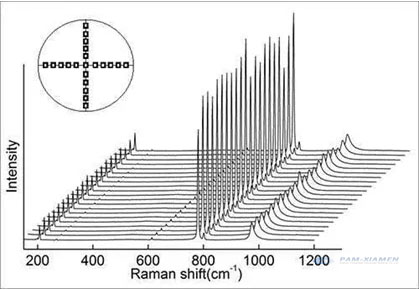
The data has three indicators: the position of the peak, the height of the peak (light intensity), and the width of the peak. Only when the peak position is completely matched, can it be 認定された4H-SiC。 XRDと同様に、他のピークがある場合は常に、それらは他の相の物質であり、これは欠陥です。
The difference in the position of the peak is due to the difference in the energy of the phonons brought about by the different silicon carbide crystal lattices, that is, the different frequencies. Each phonon has its corresponding energy level. The virtual energy level theory can be used to explain Raman (non-linear process):
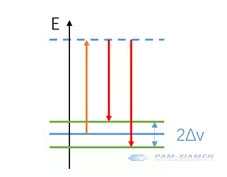
粒子は入射光を仮想エネルギーレベル(オレンジ)に吸収し、その後、元のエネルギーレベルとは異なる振動エネルギーレベル(赤)に戻ります。 上限エネルギーレベルは仮想エネルギーレベルであるため、元の実際のエネルギーレベルと競合しない限り、入射光の周波数を変えることができます。
LOPCモード(964.769 cm-1)を使用してキャリア濃度を分析できることは注目に値します。
n = 1.25 * 1017cm-2 *(964.769cm-1-VLOPC measurement)
As the carrier concentration increases, the interaction between atoms and the lattice increases, which makes the Raman peak blue shift (smaller), the intensity decreases, and the width increases. This method is not as accurate as other methods and can only be used as an aid to analyze the silicon carbide crystal distribution.
3. Why not Use XRD to Measure Silicon Carbide Crystal Distribution?
X-rays are optical radiation generated by the transition of electrons in the inner layer of atoms under the bombardment of high-speed moving electrons, including continuous X-rays and characteristic X-rays. Silicon carbide single crystal can be used as X-ray gratings, and the coherent scattering produced by these large numbers of particles (atoms, ions, or molecules) will cause light interference, increasing or decreasing the intensity of scattered X-rays. Due to the superposition of scattered waves from a large number of particles, the beams that interfere with each other to produce the highest intensity are called X-ray diffraction lines.
回折条件を満たすために、ブラッグの式を適用することができます:2dsinθ=nλ。
入射ビームにより、各散乱体はその強度のごく一部を球面波として再放射します。 散乱体が間隔dで対称に配置されている場合、これらの球面波は、光路長の差2dsinθが波長λの整数倍に等しい方向にのみ同期されます。 この場合、入射ビームの一部が2θの角度で偏向され、回折パターンに反射点が生成されます。
Use X-rays of known wavelengths to measure the θ angle to calculate the interplanar spacing d, which is used for X-ray structure analysis; the other is to use a silicon carbide seed crystal with a known d to measure the θ angle to calculate the characteristic X-ray wavelength, and then the elements contained in the sample can be found in the existing data.
The measurement formula is 2dSinθ=λ. While the d value among the cubic silicon carbide crystal is close, and the characteristic is not obvious enough, the accurate silicon carbide crystal distribution cannot be precisely determined. For these reasons, it is not suitable to use the XRD to measure the distribution of silicon carbide crystals.

詳細については、メールでお問い合わせください。 victorchan@powerwaywafer.com と powerwaymaterial@gmail.com.