PAM-XIAMEN is an expert of LED wafers, and we offer LED wafers (link: https://www.powerwaywafer.com/gan-wafer/epitaxial-wafer.html) and technology support for you on LED fabrication by our rich experience. Here we share a method of laser for scribing LED wafers. Laser processing is to irradiate a laser beam to the surface of the work piece, and use the high energy of the laser to cut, melt the material and change the surface properties of the object.
1. What Is the Laser Suitable for Scribing of LED Wafers?
With the expansion of the market, higher requirements are put forward for improving productivity and finished product qualification rate of LEDs, coupled with the rapid popularization of laser processing, laser processing has gradually become the mainstream process in the processing of sapphire for high-brightness LEDs.
However, not all lasers are suitable for LED scribing due to the transparency of the wafer material for visible wavelength lasers. GaN is transmissive for light with wavelengths less than 365nm, while sapphire wafers are semi-transmissive for lasers with wavelengths greater than 177nm. Therefore, the triple and quadruple frequency-switched Q-switched all-solid-state lasers (DPSSL) with wavelengths of 355nm and 266nm are the best choice for laser scribing of LED wafers.
2. Advantages of Scribe LED Wafers with Laser
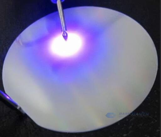
Laser processing is non-contact processing. As an alternative to traditional mechanical saw blade cutting, the laser scribing incision is very small, and the surface of the wafer under the action of the focused laser micro-spot quickly vaporizes the material, making very small LED active areas, so that more LED monomers can be cut on a wafer with limited area.
In addition, laser scribing is particularly good at sapphire, gallium nitride (GaN), gallium arsenide (GaAs) and other brittle semiconductor wafer materials. Laser processing LED wafers, the typical scribing depth is 1/3 to 1/2 of the thickness of the substrate, so that a clean fracture surface can be obtained by dividing, making narrow and deep laser scribing cracks while ensuring high-speed scribing speed. Therefore, the laser is required to have excellent quality such as narrow pulse width, high beam quality, high peak power, and high repetition frequency.
The laser scribed LED scribed lines are much narrower than the traditional mechanical scribes, so the material utilization rate is significantly improved, thus improving the output efficiency. Moreover, laser scribing brings less micro-cracks and other damage to the wafer. This makes the wafer particles closer together, resulting in high output efficiency and high productivity, while the reliability of the finished LED device is also greatly improved.

For more information, please contact us email at victorchan@powerwaywafer.com and powerwaymaterial@gmail.com.