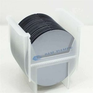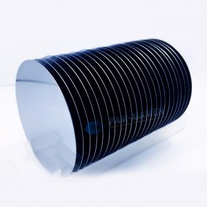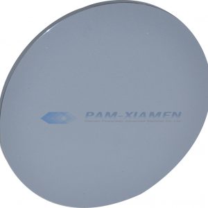
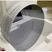
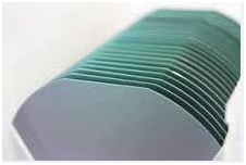
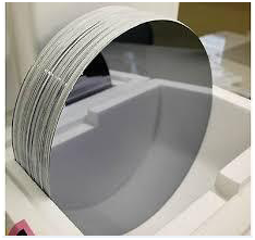
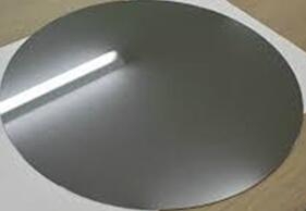
エピタキシャルシリコンウェーハ
シリコンエピタキシャルウェーハ(エピウェーハ)は、単結晶シリコンウェーハ上に堆積されたエピタキシャルシリコン単結晶の層です(注:高濃度にドープされた単結晶シリコンウェーハの上に多結晶シリコン層の層を成長させることもできますが、それはバルク Si 基板と最上部のエピタキシャル シリコン層の間にバッファ層 (酸化物またはポリ Si など) が必要であり、薄膜トランジスタにも使用できます。
- 説明
製品の説明
エピタキシャルシリコンウェーハ
シリコンエピタキシャルウェハ(エピウエハ)単結晶上に堆積されたエピタキシャル シリコン単結晶の層です。シリコンウエハ(注: 高ドープ単結晶シリコンウェーハの上に多結晶シリコン層を成長させることは可能ですが、バルク Si 基板と上部エピタキシャル層の間にバッファ層 (酸化物またはポリ Si など) が必要ですシリコン層であり、薄膜トランジスタにも使用できます。
エピタキシャルシリコンウェーハの作製方法には、気相エピタキシー、液相エピタキシー、分子線エピタキシー等がある。 中でも、化学気相成長法 (CVD) をベースとした気相成長法がシリコンエピタキシャル成長プロセスの主流となっています。 一般的に使用されるソースは、SiCl4、SiHCl3、SiH2Cl2、SiH4 です。
さまざまな半導体デバイスのニーズを満たすために、エピタキシャルシリコンウェーハを製造するためのさまざまなシリコンエピタキシャル技術が生み出されてきました。 シリコンエピタキシャル成長には、低温エピタキシャル成長や減圧エピタキシャル成長のほかに、シリコンウェーハの特定の部分にシリコンエピタキシャル層を堆積させる選択エピタキシャル成長もあります。
基板の結晶構造を継続しながら、それが正確なドーピング濃度に、堆積されるエピタキシャル層をドープすることができます。
エピ層の抵抗:150オームcmへ<1オームセンチアップ
エピ層の厚さ:<1 umの150までのUM
構造:N / N +、N- / N / N +、N / P / N +、N / N + / P-、N / P / P +、P / P +、P- / P / P +。
ウエハアプリケーション:デジタル、リニア、パワー、MOS、BiCMOSのデバイス。
一目で私たちの利点
1.高度なエピタキシャル成長装置、テスト装置およびエピタキシャルシリコン技術。
低欠陥密度と良好な表面粗さを持つ最高品質2.Offer。
当社の顧客のための研究チームのサポートと技術サポートを3.Strong
6」(150ミリメートル)ウェーハ仕様:
| アイテム | 仕様 | |
| 基板 | サブスペック号 | |
| インゴット成長方法 | CZ | |
| 導電型 | N | |
| ドーパント | として | |
| 方向付け | (100)が0.5°、±します | |
| 抵抗率 | ≤0.005Ohm.cm | |
| RRG | ≤15% | |
| [大井]コンテンツ | 8〜18 PPMA | |
| 直径 | 150±0.2ミリメートル | |
| プライマリフラット長 | 55〜60ミリメートル | |
| プライマリフラット場所 | {110}±1° | |
| 第二にフラット長 | セミ | |
| 第二にフラット場所 | セミ | |
| 厚さ | 625±15ええと | |
| 特性の裏側: | ||
| 1、BSD /ポリ-Si(A) | 1.BSD | |
| 2、SIO2 | 2.LTO:500 A±5000 | |
| 3、エッジ除外 | 3.EE:?0.6ミリメートル | |
| レーザーマーキング | 無し | |
| 前面 | 鏡面研磨 | |
| エピ | 構造 | N / N + |
| ドーパント | フォス | |
| 厚さ | 3±0.2μmの | |
| Thk.Uniformity | ≤5% | |
| 測定位置 | エッジから中心(1点)10ミリメートル(90度@ 4つのPTS) | |
| 計算 | 【のTmax-Tminを〕÷〔のTmax + Tminの] X 100% | |
| 抵抗率 | 2.5±0.2 Ohm.cm | |
| Res.Uniformity | ≤5% | |
| 測定位置 | エッジから中心(1点)10ミリメートル(90度@ 4つのPTS) | |
| 計算 | [さRmax-Rminの]÷[さRmax + Rminの] X 100% | |
| スタック欠陥密度 | ≤2(EA / cm 2)を | |
| ヘイズ | 無し | |
| 傷 | 無し | |
| クレーター、オレンジピール、 | 無し | |
| エッジクラウン | ≤1/ 3エピ厚さ | |
| スリップ(ミリメートル) | 全長≤1Dia | |
| 異物 | 無し | |
| 裏面の汚染 | 無し | |
| 合計点欠陥(粒子) | ≤30@0.3um |
あなたも好きかも...
-
GaN系テンプレート
PAM-厦門のテンプレート製品(窒化ガリウム)GaNテンプレート、(窒化アルミニウム)の結晶層からなるAlNテンプレート、(窒化アルミニウムガリウム)のAlGaNテンプレートとサファイア上に堆積される(窒化インジウムガリウム)のInGaNテンプレート -
ポリッシュウェーハ
PAM-XIAMEN は、<100>、<110>、または <111> の配向を持つ、n 型または p 型の研磨ウェハを提供できます。 FZ研磨ウェーハ、主にシリコン整流器(SR)、シリコン制御整流器(SCR)、ジャイアントトランジスタ(GTR)、サイリスタ(GRO)の製造用
-
SiCのエピタキシー
我々は、カスタム薄膜(シリコンカーバイド)、炭化ケイ素デバイスの開発のため6H又は4H基板上のSiCエピタキシーを提供します。 SiCエピタキシャルウェハは、主にショットキーダイオード、金属酸化膜半導体電界効果トランジスタ、接合型電界効果のために使用されます -
エッチングウェハ
PAM-XIAMENが提供するエッチングシリコンウェーハは、低粗さ、低反射率、高反射率を備えたN型またはP型エッチングウェーハです。 エッチングウェーハは、粗さが少なく、光沢が良く、比較的安価であるという特徴があり、一部の分野では電子素子の製造において比較的コストの高い研磨ウェーハやエピタキシャルウェーハを直接代替し、コストを低減することができる。
-
テストウェーハモニターウェーハダミーウェハ
PAM-XIAMENはダミーウェーハメーカーとして、生産装置に使用され、生産工程初期の安全性向上や納期確認、工程形状の評価に使用されるシリコンダミーウェーハ/テストウェーハ/モニターウェーハを提供しています。 ダミーシリコンウェーハは実験やテストに使用されることが多いため、そのサイズと厚さが重要な要素となることが多い。 100mm、150mm、200mm、300mmのダミーウエハをご用意しております。
-
GaAsのエピウェーハ
PAM-XIAMEN は、MBE または MOCVD によって成長させた Ga、Al、In、As、および P に基づいて、さまざまなタイプのエピ ウェーハ III-V シリコン ドープ n 型半導体材料を製造しています。 お客様の仕様を満たすカスタム GaAs エピウェーハ構造を提供します。詳細については、お問い合わせください。
-
CZ単結晶シリコン
単結晶バルクシリコン生産会社であるPAM-XIAMENは、CZ法で成長させたN&Pドーパントを含む76.2~200mmの単結晶シリコンウェーハ<100>、<110>、<111>を提供できます。 チョクラルスキー法とは、CZ法と呼ばれる結晶成長法の一つである。 直管加熱システムに組み込まれており、黒鉛抵抗によって加熱され、高純度石英るつぼに入ったポリシリコンを溶解し、その融液の表面に種結晶を挿入して溶接します。 その後、回転している種結晶を下降させて溶かします。 ボディを浸し、触り、徐々に引き上げ、ネッキング、ネッキング、ショルダリング、等径管理、仕上げの工程を経て仕上げまたは引き抜きを行います。
-
フロートゾーン単結晶シリコン
PAM-XIAMENでは、フロートゾーン法により得られるフロートゾーンシリコンウェーハを提供できます。 単結晶シリコンロッドはフロートゾーン成長によって得られ、その後、単結晶シリコンロッドをフロートゾーンシリコンウェーハと呼ばれるシリコンウェーハに加工します。 フローティングゾーンシリコンプロセス中、ゾーンメルトシリコンウェーハは石英るつぼと接触していないため、シリコン材料は浮遊状態にあります。 これにより、シリコンのフローティングゾーン溶解プロセス中の汚染が少なくなります。 炭素含有量と酸素含有量が低く、不純物が少なく、抵抗率が高くなります。 パワーデバイスや特定の高電圧電子デバイスの製造に適しています。


関連製品
-
12インチのテストグレードシリコンウェーハ
PAM-XIAMEN は、300 mm ベア シリコン ウェーハ (12 インチ) ダミー、テスト グレード、n タイプまたは p タイプを提供しています。 他のシリコンウェーハサプライヤーと比較して、Powerway Wafer は競争力のある価格でプロフェッショナルなサービスを提供します。
-
12インチプライムグレードシリコンウェーハ
PAM-XIAMEN は、プライム グレード、n タイプまたは p タイプの 300 mm ベア シリコン ウェーハ (12 インチ) を提供しています。300 mm シリコン ウェーハの厚さは 775±15 です。 他のシリコンウェーハサプライヤーと比較して、Powerway Wafer のシリコンウェーハの価格はより競争力があり、高品質です。 300mm シリコン ウェーハは、従来の大口径シリコン ウェーハよりもウェーハあたりの歩留まりが高くなります。
-
12インチシリコンウェーハ 300mm TOX (Si熱酸化ウェーハ)
PAM-XIAMEN は 300mm の酸化ケイ素ウェハーと二酸化ケイ素ウェハーを提供しています。 熱酸化シリコンウェーハまたは二酸化シリコンウェーハは、ドライまたはウェット酸化プロセスによって成長した酸化物層を備えたベアシリコンウェーハです。 シリコンウェーハの熱酸化層は通常、横型管状炉で成長し、シリコンウェーハの酸化温度範囲は一般に900℃〜1200℃です。 CVD酸化層と比較して、シリコンウェーハ酸化層は均一性が高く、緻密性が高く、絶縁耐力が高く、品質が優れています。