Gartner: worldwide semiconductor revenue declined 2.3% in 2015
Worldwide semiconductor revenue totaled 334.8 billion dollar in 2015, a 2.3 percent decline from 2014, according to final results by Gartner. The combined revenue of the top 25 semiconductor vendors fell by 0.5 percent during 2015. This was [...]
2016-07-04メタ著者
Silicon wafers with various metal depositions are for sale in sizes from 2 inch to 12 inch. Metal deposition on silicon wafer is usually processing on the substrate surface, and thickness of the substrate typically is 300um~700um. A wafer list is shown below for [...]
2021-10-13メタ著者
InGaAs/InAlAs heterostructure is realized on GaAs substrate. This GaAs-based metamorphic high electron mobility transistor (mHEMT) heterostructure can reduce the stress at the interface between heterostructure and GaAs through the gradual change of In composition. Such a mHEMT structure can provide device performance that is [...]
PAM XIAMEN offers Quartz Frit.
1” Diameter Porous Quartz Frits with Optional Porosity, 1 pc
Specifications
Diameter – mm
25
Thickness – mm
4
Porosity
15~40um or 4~15um (Please select the pore size in the optional bar)
For more information, please visit our website: https://www.powerwaywafer.com,
send us email at sales@powerwaywafer.com [...]
2019-04-18メタ著者
PAM-XIAMEN, one of LED wafer manufacturers, offers GaN Wafer for Fabricating LED Devices, which is GaN Epi Structure with InGaN MQWs on sapphire substrate, and can be blue or green emission:
1. Specification of GaN Wafer for LED Devices
No1. PAM200614-GAN-LED
size : 2 inch
WD : 455 ± 10nm
[...]
2020-06-02メタ著者
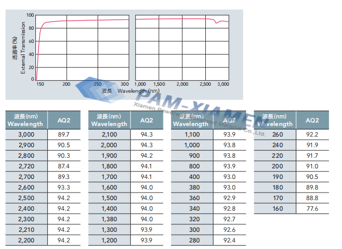
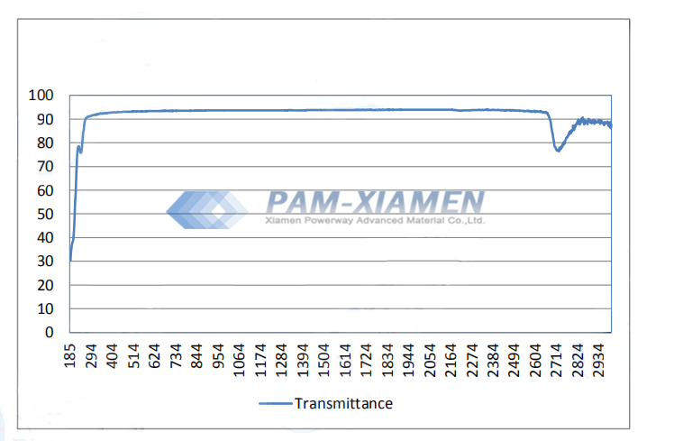
IR Transmittance Report
A test report is necessary to show the compliance between custom description and our final wafers data. We will test the wafer characerization by equipment before shipment, testing surface roughness by atomic force microscope, type by Roman spectra instrument, resistivity by non-contact [...]
2018-08-14メタ著者