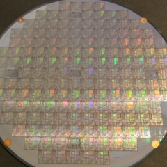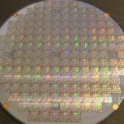
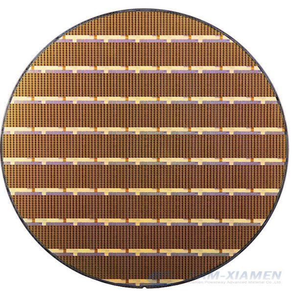
Wafer Foundry Services
PAM-XIAMEN は、高度な半導体プロセス技術を使用したウェーハ ファウンドリ サービスを提供し、基板とウェーハのエクスパキシの上流での経験から恩恵を受けます。
PAM-XIAMEN は、ファブレス企業、IDM、研究者向けに最先端のウェーハ技術とファウンドリ サービスを提供します。
- Description
製品説明
PAM-XIAMEN は、半導体製造におけるウェーハ ファウンドリ サービスを提供しています。
高度な半導体プロセス技術に感謝し、基板とウェーハの製造における上流の経験から恩恵を受けます。
PAM-XIAMEN は、ファブレス企業、IDM、研究者向けに最先端のウェーハ技術とファウンドリ サービスを提供します。
現在、微細加工用の200mmウェーハ製造施設(fab)があります。
ウェーハファウンドリサービス
| プロジェクト名 | Wafergroße (Zoll) | フェーヒケイト |
| シュリットフォトリソグラフィー | 6 | 0.40μm |
| フォトリソグラフィーの問い合わせ | 2,4 | 3um |
| トロッケネッツェン | 6 | Tiefe 100 um (Si)、メタル、GaN |
| ナッセ銀行 | 6,8 | 金属、SiO 2 、SiN、TEOS、ポリシリコン |
| PECVD | 6 | SiN SiO2.TEOS |
| LPCVD | 6 | SiN、SiO2、ポリシリジウム |
| ALD | 6 | Al2O3、AIN |
| スパッターン | 6 | Ti.Al、TiN、Ni、W.TiW.WN |
| エレクトロネンシュトラール | 4,6,8 | チタン、ニッケル、銀。 Al.Ta、Cr Pt.Mo、Co. |
| 移植 | 6 | B (20 – 200 KeV、1E13 – 115) .N |
| RTP | 6 | 最大900℃ |
| バックオーフェン | 6 | 最大400℃ |
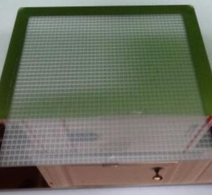
ウェーハ製造のファウンドリサービス機能は次のとおりです。
最大8インチの金属プロセス:スパッタシステムまたはEビームシステムによるTi、Ni、Ag、Pt、Mo、Al、W、Crなどによるウェーハメタライゼーション
ALM、SAMCO RIE、またはICPエッチング装置による最大6インチのドライエッチングプロセス
フィルムプロセス:PECVD、DF&LPCVD、ALDおよびUnitempRTPによるSiO2、SiN、Al2O3薄膜。
4. 2″ / 4″ / 6″のリソグラフィープロセス:最小。 ニコンステッパーによる線幅0.4um
投影リソグラフィー:CD 2um、精度1um
ULVACによる2″ / 4″ / 6″用のイオン注入装置(B +、BF2 +、P +、As +、Ar +、B ++、P ++)
ウェーハ製造プロセスは、生のウェーハを完成したチップに加工するために行われます。
従来のウェーハ製造プロセスには、抵抗器、トランジスタ、導体、
および半導体ウェーハ上で処理するその他の電子部品。
ナノリソグラフィー(フォトリソグラフィー)を提供できます:表面処理、フォトレジスト塗布、ソフトベイク、
アライメント、露光、現像、ハードベーク、現像検査、エッチング、フォトレジスト除去(ストリップ)、最終検査。
詳細については、当社の Web サイトをご覧ください。https://www.powerwaywafer.com/wafer-fabrication
にメールを送ってくださいsales@powerwaywafer.com と powerwaymaterial@gmail.com
関連製品
-
ナノファブリケーションフォトレジスト
PAM-XIAMENフォトレジスト付きフォトレジストプレートを提供
-
フォトマスク
PAM-厦門オファーフォトマスク
フォトマスクは、厚い基板に支えられたマスキング材の薄いコーティングであり、マスキング材はさまざまな程度で光を吸収し、カスタムデザインでパターン化できます。 パターンは、光を変調し、フォトリソグラフィのプロセスを通じてパターンを転写するために使用されます。フォトリソグラフィは、今日のほとんどすべてのデジタルデバイスを構築するために使用される基本的なプロセスです。