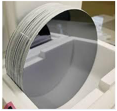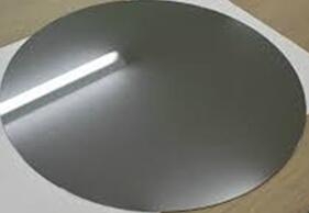
12 ″ 프라임 그레이드 실리콘 웨이퍼
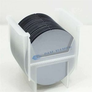
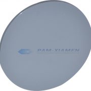
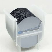
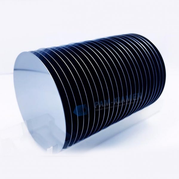
PAM-XIAMEN offer 300mm bare silicon wafers (12 inch) in prime grade, n type or p type, and the 300mm silicon wafer thickness is 775±15. Compared to other silicon wafer suppliers, Powerway Wafer’s silicon wafer price is more competitive with higher quality. 300mm silicon wafers have a higher yield per wafer than pervious large diameter silicon wafers.
- 기술
제품 설명
PAM-XIAMEN offer 300mm bare silicon wafers (12 inch) in prime grade, n type or p type, and the 300mm silicon wafer thickness is 775±15. Compared to other silicon wafer suppliers, Powerway Wafer’s silicon device wafer price is more competitive with higher quality. 300mm silicon wafers have a higher yield per wafer than pervious large diameter silicon wafers. Size on/above 8 inches (200 mm) is called a large silicon wafer. The production technology of large silicon wafer is not only the increase of process complexity because of the increase of area, but also the higher requirements on many other control factors. For example: oxygen content and its radial uniformity in wafer, impurity control, OISF control, etc. The silicon wafer requirements for defect control, oxygen precipitation control, resistance quantification, doping and radial uniformity are also higher. Especially for prime grade 300mm silicon wafer, some parameters are required critically, for instant, wafer TTV is below1.5um and defect density ~0/cm2. The next step is 450mm silicon ingot or wafer.
1. Parameters of 300mm Silicon Wafer
| 매개 변수 | Value(PAM210512-300-SIL) |
| 잉곳의 종류 | 초크 랄 스키 법에 의해 성장한 |
| Diametr, mm | 300 ± 0.2 |
| 도펀트 | B (붕소) |
| 도전 형 | P |
| Oxigen 최대, OLD-PPMA | 40 |
| 탄소, PPMA | 1 |
| 결정 방위 | <100> |
| 결정면의 미리 결정된 표면 방향 편차, deg | 1 |
| 볼륨 저항, 옴 · cm | 8-12 |
| 차 노치 | 예 |
| 노치 위치 | 110 |
| 노치 크기, mm | 2,3 |
| 노치 양식 | V |
| 웨이퍼 두께, 마이크론 | 775 ± 15 |
| 마킹의 종류 | 레이저 |
| 표시 위치 | 후면 |
| 에지 프로필 | SEMI T / 4 제작 |
| 앞면의 긁힘 | 결석 |
| 전면 연마 | 예 |
| 뒷면 연마 | 예 |
| 웨이퍼 두께 (TTV)의 총 변화, 마이크로 미터 | 1,5 |
| 처짐 (WARP), 미크론 | 30 |
| 0.05 미크론보다 큰 표면의 입자 수 | 50 |
| 0.09 미크론보다 큰 표면의 입자 수 | 30 |
| 알루미늄 표면 콘텐츠 E10AT / CM2 | 1 |
| 칼슘의 표면 내용, E10AT / CM2 | 1 |
| 크롬의 표면 내용, E10AT / CM2 | 1 |
| 구리의 표면 내용, E10AT / CM2 | 1 |
| 철의 표면 내용, E10AT / CM2 | 1 |
| 칼륨의 표면 내용, E10AT / CM2 | 1 |
| 나트륨의 표면 내용, E10AT / CM2 | 1 |
| 니켈 표면 콘텐츠 E10AT / CM2 | 1 |
| 아연, E10AT / CM2의 표면 내용 | 1 |
요구 사항을 포장 :
| 매개 변수 | |
| 포장의 종류 | MW300GT-A |
| 내부 용기 재질 | 폴리에틸렌 |
| 외부 포장 재료 | 알루미늄 |
| 하나 개의 패키지에서 조각의 수 | 25 |
| 재사용 성 | 예 |
2. FAQ:
Q: Please take note that we offer “The number of particles on a surface larger than 0.09 microns 50” just for silicon substrate.
일반적으로 입자 요구 사항은 실리콘 기판입니다.
규정 준수를 확인하기 위해 확인해 주시겠습니까?
A: 다시 한 번 확인했습니다. 예, 표시된 정보가 정확합니다.
PAM-XIAMEN은 기술 및 웨이퍼 지원을 제공 할 수 있습니다.
자세한 내용은 저희 웹 사이트를 방문하십시오 :https://www.powerwaywafer.com/silicon-wafer,
에서 우리에게 이메일을 보내sales@powerwaywafer.com및powerwaymaterial@gmail.com
관련 제품
-
광택 웨이퍼
PAM-XIAMEN can offer polished wafer, n type or p type with orientation at <100>, <110> or <111>. FZ polished wafers, mainly for the production of silicon rectifier (SR), silicon controlled rectifier (SCR), Giant Transistor (GTR), thyristor (GRO)
-
CZ 단결정 실리콘
PAM-XIAMEN, a monocrystalline bulk silicon producer, can offer <100>, <110> and <111> monocrystalline silicon wafers with N&P dopant in 76.2~200 mm, which are grown by CZ method. The Czochralski method is a crystal growth method, referred to as the CZ method. It is integrated in a straight-tube heat system, heated by graphite resistance, melts the polysilicon contained in a high-purity quartz crucible, and then inserts the seed crystal into the surface of the melt for welding. After that, the rotating seed crystal is lowered and melted. The body is infiltrated and touched, gradually raised, and finished or pulled through the steps of necking, necking, shouldering, equal diameter control, and finishing.
-
테스트 웨이퍼 모니터 웨이퍼 더미 웨이퍼
PAM-XIAMEN은 더미 웨이퍼 제조업체로서 생산 공정 초기에 안전성을 향상시키기 위해 생산 장치에 사용되는 실리콘 더미 웨이퍼/테스트 웨이퍼/모니터 웨이퍼를 제공하고, 납품 확인 및 공정 형태 평가에 사용됩니다. 더미 실리콘 웨이퍼는 실험이나 테스트용으로 많이 사용되기 때문에 대부분의 경우 그 크기와 두께가 중요한 요소입니다. 100mm, 150mm, 200mm 또는 300mm 더미 웨이퍼를 사용할 수 있습니다.
-
에칭 웨이퍼
The etching silicon wafers offered by PAM-XIAMEN are N type or P type etching wafers, which have low roughness, low reflectivity and high reflectivity. The etching wafer has the characteristics of low roughness, good glossiness and relatively low cost, and directly substitutes the polished wafer or epitaxial wafer which has relatively high cost to produce the electronic elements in some fields, reducing the costs.
-
플로트 존 단결정 실리콘
PAM-XIAMEN은 Float Zone 방식으로 얻은 플로트 존 실리콘 웨이퍼를 제공할 수 있습니다. 단결정 실리콘 로드는 플로트 존 성장을 통해 얻은 다음 단결정 실리콘 로드를 플로트 존 실리콘 웨이퍼라고 하는 실리콘 웨이퍼로 가공합니다. 플로팅 존 실리콘 공정 동안 존 용융 실리콘 웨이퍼는 석영 도가니와 접촉하지 않기 때문에 실리콘 재료는 부유 상태에 있게 된다. 이로써 실리콘의 플로팅 존 용융 과정에서 오염이 덜합니다. 탄소 함량과 산소 함량은 더 낮고 불순물은 적으며 저항률은 더 높습니다. 전력 장치 및 특정 고전압 전자 장치의 제조에 적합합니다.
-
에피 택셜 실리콘 웨이퍼
Silicon Epitaxial Wafer(Epi Wafer) is a layer of epitaxial silicon single crystal deposited onto a single crystal silicon wafer(note: it is available to grow a layer of poly crystalline Silicon layer on top of a highly doped Singly crystalline silicon wafer, but it needs buffer layer (such as oxide or poly-Si) in between the bulk Si substrate and the top epitaxial silicon layer. It also can be used for thin film transistor.
-
12 "실리콘 웨이퍼 300mm TOX (열 산화 실리콘 웨이퍼)
PAM-XIAMEN offers 300mm silicon oxide wafer and dioxide wafer. Thermal oxide silicon wafer or silicon dioxide wafer is a bare silicon wafer with oxide layer grown by dry or wet oxidation process. The thermal oxide layer of the silicon wafer is usually grown in a horizontal tube furnace, and the silicon wafer oxide temperature range is generally 900 ℃ ~ 1200 ℃. Compared with CVD oxide layer, silicon wafer oxide layer has higher uniformity, better compactness, higher dielectric strength and better quality.
-
12 "테스트 학년 실리콘 웨이퍼
PAM-XIAMEN offers 300mm bare silicon wafers (12 inch) dummy, test grade, n type or p type. Compared to other silicon wafer suppliers, Powerway Wafer offers professional service with competitive prices.