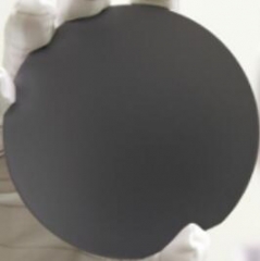

GaN 계 LED 에피 택셜 웨이퍼
PAM-XIAMEN의 질화 갈륨 (질화 갈륨) LED 에피 택셜 웨이퍼는 초 고휘도 청색 및 녹색 발광 다이오드 (LED) 및 레이저 다이오드 (LD) 기반 애플리케이션이다.
- 기술
제품 설명
The LED epitaxial wafer is a substrate heated to an appropriate temperature. The LED wafer material is the cornerstone of the technology development for the semiconductor lighting industry. Different substrate materials require different LED epitaxial wafer growth technology, chip processing technology and device packaging technology. The substrate for LED epi wafer determines the development route of semiconductor lighting technology. To achieve luminous efficiency, epitaxial wafer suppliers pay more attention to GaN based LED epitaxial wafer, since the epitaxial wafer price is in low cost, and the epi wafer defect density is small. LED epi wafer advantage on GaN substrate is the realization of high efficiency, large area, single lamp and high power, which make the process technology simplify and improve the large yield rate. The development prospects of the LED epi wafer market are optimistic.
1. LED Wafer List
|
LED Epitaxial Wafer |
||||||||
| Size | Orientation | Emission | Wavelength | Thickness | 기판 | Surface | Usable area | |
| PAM-50-LED-BLUE-F | 50mm | 0°±0.5° | blue light | 445-475nm | 425um+/-25um | Sapphire | P/L | >90% |
| PAM-50-LED-BLUE-PSS | 50mm | 0°±0.5° | blue light | 445-475nm | 425um+/-25um | Sapphire | P/L | >90% |
| PAM-100-LED-BLUE-F | 100mm | 0°±0.5° | blue light | 445-475nm | / | Sapphire | P/L | >90% |
| PAM-100-LED-BLUE-PSS | 100mm | 0°±0.5° | blue light | 445-475nm | / | Sapphire | P/L | >90% |
| PAM-150-LED-BLUE | 150mm | 0°±0.5° | blue light | 445-475nm | / | Sapphire | P/L | >90% |
| PAM-100-LED-BLUE-SIL | 50mm | 0°±0.5° | blue light | 445-475nm | / | Silicon | P/L | >90% |
| PAM-100-LED-BLUE-SIL | 100mm | 0°±0.5° | blue light | 445-475nm | / | Silicon | P/L | >90% |
| PAM-150-LED-BLUE-SIL | 150mm | 0°±0.5° | blue light | 445-475nm | / | Silicon | P/L | >90% |
| PAM-200-LED-BLUE-SIL | 200mm | 0°±0.5° | blue light | 445-475nm | / | Silicon | P/L | >90% |
| PAM-50-LED-GREEN-F | 50mm | 0°±0.5° | green light | 510-530nm | 425um+/-25um | Sapphire | P/L | >90% |
| PAM-50-LED-GREEN-PSS | 50mm | 0°±0.5° | green light | 510-530nm | 425um+/-25um | Sapphire | P/L | >90% |
| PAM-100-LED-GREEN-F | 100mm | 0°±0.5° | green light | 510-530nm | / | Sapphire | P/L | >90% |
| PAM-100-LED-GREEN-PSS | 100mm | 0°±0.5° | green light | 510-530nm | / | Sapphire | P/L | >90% |
| PAM-150-LED-GREEN | 150mm | 0°±0.5° | green light | 510-530nm | / | Sapphire | P/L | >90% |
| PAM-100-LED-RED-GAAS-620 | 100mm | 15°±0.5° | red light | 610-630nm | / | 갈륨 비소 | P/L | >90% |
| PAM210527-LED-660 | 100mm | 15°±0.5° | red light | 660nm | / | 갈륨 비소 | P/L | >90% |
| PAM-210414-850nm-LED | 100mm | 15°±0.5° | IR | 850nm | / | 갈륨 비소 | P/L | >90% |
| PAMP21138-940LED | 100mm | 15°±0.5° | IR | 940nm | / | 갈륨 비소 | P/L | >90% |
| PAM-50-LED-UV-365-PSS | 50mm | 0°±0.5° | UVA | 365 nm | 425um+/-25um | Sapphire | ||
| PAM-50-LED-UV-405-PSS | 50mm | 0°±0.5° | UVA | 405 nm | 425um+/-25um | Sapphire | ||
| PAM-50-LED-UVC-275-PSS | 50mm | 0°±0.5° | UVC | 275nm | 425um+/-25um | Sapphire | ||
| PAM-50-LD-UV-405-SIL | 50mm | 0°±0.5° | UV | 405nm | / | Silicon | P/L | >90% |
| PAM-50-LD-BLUE-450-SIL | 50mm | 0°±0.5° | blue light | 450nm | / | Silicon | P/L | >90% |
As a LED epitaxial wafer manufacturer, PAM-XIAMEN can offer activated and unactivated GaN Epi LED wafer for LED and laser diodes (LD) application,such as For micro LED or ultra thin wafer or UV LED researches or LED manufacturers. LED epitaxial wafer on GaN is grown by MOCVD with PSS or flat sapphire for LCD back light, mobile, electronic or UV(ultraviolet), with blue or green or red emission, including InGaN/GaN active area and AlGaN layers with GaN well/AlGaN barrier for different chip sizes.
2. InGaN/질화 갈륨(gallium nitride) based LED Epitaxial Wafer
GaN으로 Al2O3-2에 "에피 웨이퍼 사양 (LED 에피 택셜 웨이퍼)
| White: 445~460 nm |
| Blue: 465~475 nm |
| Green: 510~530 nm |
1. 성장 기술 - MOCVD
2.Wafer 직경 :이 50.8mm
3.Wafer substrate material: Patterned Sapphire Substrate(Al2O3) or Flat Sapphire
4.Wafer 패턴의 크기 : 3X2X1.5μm
3. Wafer structure:
| 구조 층 | Thickness(μm) |
| p 형 질화 갈륨 | 0.2 |
| P-AlGaN으로 | 0.03 |
| 된 InGaN / GaN으로 (활성 영역) | 0.2 |
| n 형 GaN으로 | 2.5 |
| U-의 GaN | 3.5 |
| Al2O3를 (기판) | 430 |
4. Wafer parameters to make chips:
| em | 색 | 칩 크기 | 형질 | 외관 | |
| PAM1023A01 | 블루 | 10 밀 X 23mil |  |
조명 | |
| VF = 2.8 ~ 3.4V | LCD 백라이트 | ||||
| 포 = 18 ~ 25MW | 모바일 기기 | ||||
| WD = 450 ~ 460 ㎚ | 소비자 전자 | ||||
| PAM454501 | 블루 | X 45mil 45mil | VF = 2.8 ~ 3.4V |  |
일반 조명 |
| 포 = 250 ~는 300mW | LCD 백라이트 | ||||
| WD = 450 ~ 460 ㎚ | 야외 디스플레이 |
5. Application of LED epitaixal wafer:
*If you need to know more detail information of Blue LED Epitaxial Wafer, please contact with our sales departments
조명
LCD 백라이트
모바일 기기
소비자 전자
6. Specification of LED Epi Wafer as an example:
Spec PAM190730-LED
– size : 4 inch
– WD : 455 ± 10nm
– brightness : > 90mcd
– VF : < 3.3V
– n-GaN Thickness : <4.1㎛
– u-GaN thickness : <2.2㎛
– substrate : patterned sapphire substrate (PSS)
7.GaAs(Gallium arsenide)based LED Wafer Material:
LED의 GaAs 웨이퍼에 관해서는, 이들이 MOCVD에 의해 성장되고, GaAs로 파장 LED 웨이퍼 아래 참조 :
레드 : 585nm 정격, 615nm, 620 ~ ~ 630㎚
Yellow:587 ~ 592nm
Yellow/Green: 568 ~ 573nm
8. Definition of LED Epitaxial Wafer:
What we offer is bare LED epi wafer or not processed wafer without lithography processes, n- and metals contacts, etc. And you can fabricate the LED chip using your fabrication equipment for different application such as nano optoelectronics research.
주목:
중국 정부는 갈륨 재료(GaAs, GaN, Ga2O3, GaP, InGaAs, GaSb 등)와 반도체 칩 제조에 사용되는 게르마늄 재료의 수출에 대한 새로운 제한을 발표했습니다. 2023년 8월 1일부터 이러한 자재의 수출은 중국 상무부로부터 허가를 받은 경우에만 허용됩니다. 여러분의 이해와 협력을 바랍니다!
웨이퍼 사양을 LED 이러한 세부 갈륨 비소를 참조하시기 바랍니다 :LED에 대한 갈륨 비소 에피 웨이퍼
UV는 웨이퍼 사양을 LED를 참조하시기 바랍니다 :UV LED 에피 웨이퍼
실리콘 사양에 LED 웨이퍼를 참조하시기 바랍니다 :실리콘에 LED 웨이퍼
블루의 GaN LD 웨이퍼 사양은 다음 페이지를 참조하세요 블루의 GaN LD 웨이퍼
For Violet GaN LD Wafer, please visit: 405nm GaN Laser Diode Wafer
850nm and 940nm infrared LED wafer
850-880nm and 890-910nm Red Infrared AlGaAs /GaAs LED Epi-Wafer
GaN Wafers to Fabricate LED Devices
GaN LED Structure Epitaxy on Flat or PSS Sapphire Substrate
Formation of V-Shaped Pits in Nitride Films Grown by Metalorganic Chemical Vapor Deposition
Si-based GaN PIN Photodetector Structure
For more foundry services, please visit: GaN Foundry Services for LED Fabrication
당신은 또한 같은 수 있습니다 ...
-
창 (게르마늄) 싱글 수정 및 웨이퍼
PAM-XIAMEN은 2", 3", 4" 및 6" 게르마늄 웨이퍼를 제공합니다. 이는 VGF/LEC에서 성장한 Ge 웨이퍼의 약자입니다. 가볍게 도핑된 P 및 N 유형 게르마늄 웨이퍼는 홀 효과 실험에도 사용할 수 있습니다. 실온에서 결정질 게르마늄은 부서지기 쉽고 가소성이 거의 없습니다. 게르마늄은 반도체 특성을 가지고 있습니다. 고순도 게르마늄에 3가 원소(예: 인듐, 갈륨, 붕소)를 도핑하여 P형 게르마늄 반도체를 얻습니다. 및 5가 원소(안티몬, 비소, 인 등)를 도핑하여 N형 게르마늄 반도체를 얻습니다. 게르마늄은 높은 전자 이동성과 높은 정공 이동성과 같은 우수한 반도체 특성을 가지고 있습니다. -
InSb를 웨이퍼
PAM-XIAMEN은 화합물 반도체 InSb 웨이퍼 - LEC(Liquid Encapsulated Czochralski)에 의해 n 유형, p 유형 또는 다른 방향(111) 또는 (100)의 반절연을 갖춘 Epi-Ready 또는 기계적 등급으로 성장한 안티몬화 인듐 웨이퍼를 제공합니다. 등전자로 도핑된 안티몬화인듐(예: N 도핑)은 안티몬화인듐 박막 제조 공정 중 결함 밀도를 줄일 수 있습니다.
-
의 GaN HEMT 에피 택셜 웨이퍼
Gallium Nitride (GaN) HEMTs (High Electron Mobility Transistors) are the next generation of RF power transistor technology. Thanks to GaN technology, PAM-XIAMEN now offer AlGaN/GaN HEMT Epi Wafer on sapphire or Silicon, and AlGaN/GaN on sapphire template.
-
갈륨 비소 에피 웨이퍼
PAM-XIAMEN은 MBE 또는 MOCVD로 성장한 Ga, Al, In, As 및 P를 기반으로 하는 다양한 유형의 에피 웨이퍼 III-V 실리콘 도핑 n형 반도체 재료를 제조하고 있습니다. 우리는 고객 사양을 충족하기 위해 맞춤형 GaAs 에피웨이퍼 구조를 공급합니다. 자세한 내용은 당사에 문의하십시오.
-
프리 스탠딩 GaN 기판
PAM-XIAMEN는 UHB-LED 및 LD위한 (질화 갈륨), GaN 기판 웨이퍼를 자립의 제조 기술을 확립했다. 수 소화물 기상 성장 (HVPE) 기술에 의해 성장 우리 GaN 기판은 낮은 결함 밀도를 갖는다.
-
의 GaN 템플릿
PAM-XIAMEN의 템플릿 제품은 사파이어 상에 증착된다 (질화 갈륨) 질화 갈륨 템플릿 (질화 알루미늄)의 AlN 템플릿 (질화 알루미늄 갈륨)을 AlGaN 템플릿 (인듐 갈륨 나이트 라이드)의 InGaN 템플릿의 결정질 층으로 이루어져 -
의 SiC 웨이퍼 기판
이 회사는 결정 성장, 결정 처리, 웨이퍼 처리, 연마, 세척 및 테스트를 통합하는 완전한 SiC(탄화 규소) 웨이퍼 기판 생산 라인을 보유하고 있습니다. 현재 우리는 축상 또는 축외에서 반절연 및 전도성을 갖춘 상용 4H 및 6H SiC 웨이퍼를 공급하고 있으며 사용 가능한 크기는 5x5mm2,10x10mm2, 2",3",4", 6" 및 8"입니다. 결함억제, 종자결정 가공 및 급속 성장으로 탄화규소 에피택시, 소자 등에 관한 기초 연구개발을 추진합니다.
-
CZ 단결정 실리콘
PAM-XIAMEN, a monocrystalline bulk silicon producer, can offer <100>, <110> and <111> monocrystalline silicon wafers with N&P dopant in 76.2~200 mm, which are grown by CZ method. The Czochralski method is a crystal growth method, referred to as the CZ method. It is integrated in a straight-tube heat system, heated by graphite resistance, melts the polysilicon contained in a high-purity quartz crucible, and then inserts the seed crystal into the surface of the melt for welding. After that, the rotating seed crystal is lowered and melted. The body is infiltrated and touched, gradually raised, and finished or pulled through the steps of necking, necking, shouldering, equal diameter control, and finishing.