1.Specs of AlGaInP Wafers on Chips
| Parameter | Condition | Min. | Typ. | Max. | Unit |
| Forward Voltage(Vf1) | If=10μA | 1.35 | ﹎ | ﹎ | V |
| Forward Voltage(Vf2) | If=20mA | ﹎ | ﹎ | 2.2 | V |
| Reverse Voltage(Lr) | Vr=10V | ﹎ | ﹎ | 2 | μA |
| Dominant wavelength(λd) | If=20mA | 565 | ﹎ | 575 | nm |
| FWHM(Δλ) | If=20mA | ﹎ | 10 | ﹎ | nm |
| Code | LC | LD | LE | LF | LG | LH | LI |
| IV(mcd) | 20-30 | 25-35 | 30-35 | 35-50 | 40-60 | 50-70 | 60-80 |
2. Band gap of strained AlGaInP on GaAs substrate
Band parameters for III-V compound semiconductors and their alloys
I. Vurgaftman, J.R. Meyer, L.R. Ram-Mohan
J. Appl. Phys. 89 (11), 5815 (2001)
| 1)AlP | strained tensilely | with respect to GaAs |
| 2)GaP | strained tensilely | with respect to GaAs |
| 3)InP | strained compressively | with respect to GaAs |
| 4)AlxGa1-xP | strained tensilely | with respect to GaAs |
| 5)GaxIn1-xP | strained | with respect to GaAs |
| 6)AlxIn1-xP | strained | with respect to GaAs |
| 7)Al0.4Ga0.6P | strained tensilely | with respect to GaAs |
| 8)Ga0.4In0.6P | strained compressively | with respect to GaAs |
| 9)Al0.4In0.6P | strained compressively | with respect to GaAs |
| Each material layer has a length of 10 nm in the simulation. | ||
| The material layers 4), 5) and 6) vary its alloy contents linearly: | ||
| 4)AlxGa1-xP from 10 nm to 20 nm from x=0.0 to x=1.0 | ||
| 5)GaxIn1-xP from 30 nm to 40 nm from x=0.0 to x=1.0 | ||
| 6)AlxIn1-xP from 50 nm to 60 nm from x=1.0 to x=0.0 | ||
3. About AlGaInP/InGaP Structure
Since InGaAlP quaternary materials can have a wide direct band gap, by adjusting the composition of In, Al and Ga, they can be lattice-matched with high-quality and low-cost GaAs thin films. The light-emitting range of the epitaxial structure can cover red, orange, yellow, yellow-green band. Thus in the visible light emitting diode, 650nm red laser has a wide range of applications.
AlGaInP quaternary compound materials are used to grow GaAs epitaxial wafers, which are widely used in high-brightness red light emitting diodes and semiconductor lasers and have become the mainstream material for red light emitting devices. The conduction band order of AlGaInP/GaInP heterojunctions is very small, with a maximum value of about 270meV, which is smaller than that of 350meV AlGaAs materials. The electronic barrier is relatively low, and the leakage current is formed. The threshold current of the laser based GaAs epitaxy wafer is increased, which is more obvious in high temperature and high current operation. The AlGaInP layer will scatter in the alloy, and the thermal resistance is much higher than that of AlGaAs. The excess heat causes the junction temperature and cavity surface temperature. Therefore, the characteristic temperature of AlGaInP laser is lower, and the electro-optical conversion efficiency becomes lower during continuous operation, and more heat is generated.
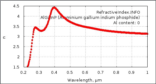
4. Refractive Index of AlGaInP
Source:PAM-XIAMEN
For more information, please contact us email at victorchan@powerwaywafer.com and powerwaymaterial@gmail.com.