


의 InAs 웨이퍼
PAM-XIAMEN은 LEC(Liquid Encapsulated Czochralski)에 의해 성장된 인듐 비소 웨이퍼인 화합물 반도체 InAs 웨이퍼를 n형, p형 또는 다른 방향(111) 또는 (100)의 반절연을 갖춘 Epi-Ready 또는 기계적 등급으로 제공합니다. 또한 InAs 단결정은 전자 이동도가 높아 홀 장치를 만드는데 이상적인 재료입니다.
- 기술
제품 설명
PAM-XIAMEN offers Compound Semiconductor InAs wafer – indium arsenide wafer which is grown by LEC(Liquid Encapsulated Czochralski) as epi-ready or mechanical grade with n type, p type or semi-insulating in different orientation(111)(100) or (110). In addition, InAs single crystal has high electron mobility and is an ideal material for making Hall devices.
Indium arsenide, InAs, is a semiconductor composed of indium and arsenic. It has the appearance of grey cubic crystals with a melting point of 942 °C and lattice constant of 0.6058nm, and the indidum arsenide crystal structure is a zinc blende structure. Indium arsenide wafer is used for construction of infrared detectors, for the wavelength range of 1–3.8 µm. The detectors are usually photovoltaic photodiodes. Cryogenically cooled detectors have lower noise, but InAs detectors can be used in higher-power applications at room temperature as well. Because of the superior indium arsenide properties, indium arsenide thin films are also used for making of diode lasers.
Indium arsenide band gap is a direct transition, which is similar to gallium arsenide, and the forbidden band width is (300K)0.45eV. Indium arsenide is sometimes used together with indium phosphide. Alloyed with gallium arsenide, it forms indium gallium arsenide – a material with band gap dependent on In/Ga ratio, a method principally similar to alloying indium nitride with gallium nitride to yield indium gallium nitride.
다음은 세부 사양은 다음과 같습니다
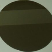
2 "(이 50.8mm)의 InAs 웨이퍼 규격
3 "(76.2mm)의 InAs 웨이퍼 규격
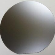
4 "(100mm)의 InAs 웨이퍼 규격
2 "의 InAs 웨이퍼 규격
| 명세서 | ||||
| 도펀트 | low doped | 태늄 | 황 | 아연 |
| 전도 유형 | N 형 | N 형 | N 형 | P 형 |
| 웨이퍼 직경 | 2 " | |||
| 웨이퍼 방향 | (111)±0.5° , (110)±0.5° | |||
| 웨이퍼 두께 | 500 ± 25um | |||
| 기본 평면 길이 | 16 ± 2mm | |||
| 차 평면 길이 | 8 ± 1mm | |||
| 캐리어 농도 | 5×1016cm-3 | (5-20)x1017cm-3 | (1-10)x1017cm-3 | (1-10)x1017cm-3 |
| 유동성 | ≥2×104cm2/V.s | 7000-20000cm2/V.s | 6000-20000cm2/V.s | 100-400cm2/V.s |
| EPD | <5×104cm-2 | <5×104cm-2 | <3×104cm-2 | <3×104cm-2 |
| TTV | <10um | |||
| 활 | <10um | |||
| 경사 | <12um | |||
| 레이저 마킹 | 요청에 따라 | |||
| Suface 마무리 | P / E, P / P | |||
| 준비 에피 | 예 | |||
| 패키지 | 단일 웨이퍼 용기 또는 카세트 | |||
3″ InAs Wafer Specification
| 명세서 | ||||
| 도펀트 | low doped | 태늄 | 황 | 아연 |
| 전도 유형 | N 형 | N 형 | N 형 | P 형 |
| 웨이퍼 직경 | 삼" | |||
| 웨이퍼 방향 | (111)±0.5° , (110)±0.5° | |||
| 웨이퍼 두께 | 600 ± 25um | |||
| 기본 평면 길이 | 22 ± 2mm | |||
| 차 평면 길이 | 11 ± 1mm | |||
| 캐리어 농도 | 5×1016cm-3 | (5-20)x1017cm-3 | (1-10)x1017cm-3 | (1-10)x1017cm-3 |
| 유동성 | ≥2×104cm2/V.s | 7000-20000cm2/V.s | 6000-20000cm2/V.s | 100-400cm2/V.s |
| EPD | <5×104cm-2 | <5×104cm-2 | <3×104cm-2 | <3×104cm-2 |
| TTV | <12um | |||
| 활 | <12um | |||
| 경사 | <15um | |||
| 레이저 마킹 | 요청에 따라 | |||
| Suface 마무리 | P / E, P / P | |||
| 준비 에피 | 예 | |||
| 패키지 | 단일 웨이퍼 용기 또는 카세트 | |||
4″ InAs Wafer Specification
| 명세서 | ||||
| 도펀트 | low doped | 태늄 | 황 | 아연 |
| 전도 유형 | N 형 | N 형 | N 형 | P 형 |
| 웨이퍼 직경 | 4 " | |||
| 웨이퍼 방향 | (111)±0.5° , (110)±0.5° | |||
| 웨이퍼 두께 | 900 ± 25um | |||
| 기본 평면 길이 | 16 ± 2mm | |||
| 차 평면 길이 | 8 ± 1mm | |||
| 캐리어 농도 | 5×1016cm-3 | (5-20)x1017cm-3 | (1-10)x1017cm-3 | (1-10)x1017cm-3 |
| 유동성 | ≥2×104cm2/V.s | 7000-20000cm2/V.s | 6000-20000cm2/V.s | 100-400cm2/V.s |
| EPD | <5×104cm-2 | <5×104cm-2 | <3×104cm-2 | <3×104cm-2 |
| TTV | <15um | |||
| 활 | <15um | |||
| 경사 | <20um | |||
| 레이저 마킹 | 요청에 따라 | |||
| Suface 마무리 | P / E, P / P | |||
| 준비 에피 | 예 | |||
| 패키지 | 단일 웨이퍼 용기 또는 카세트 | |||
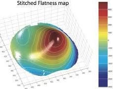
Stitched Flatness Map of InAs Wafer
Wafer Spec(example):
1) 2 '(이 50.8mm)의 InAs
Type/Dopant:N/S
Orientation:[111B]±0.5°
Thickness:500±25um
Epi-Ready
SSP
2) 2 '(이 50.8mm)의 InAs
Type/Dopant:N/low doped
Orientation : (111)B
Thickness:500um±25um
SSP
3) 2 '(이 50.8mm)의 InAs
Type/Dopant:N / low doped
Orientation : <111>A ±0.5°
Thickness:500um±25um
epi-ready
Ra<=0.5nm
Carrier Concentration(cm-3):1E16~3E16
Mobility(cm -2 ):>20000
EPD(cm -2 ):<15000
SSP
4) 2 '(이 50.8mm)의 InAs
Type/Dopant:N/low doped
Orientation : <100> with [001]O.F.
Thickness:2mm
AS cut
5) 2 '(이 50.8mm)의 InAs
Type/Dopant:N/P
Orientation :(100),
Carrier Concentration(cm-3):(5-10)E17,
Thickness:500 um
SSP
6)Indium Arsenide wafers,
2″Ø×500±25µm,
p-type InAs:Zn
(110)±0.5°,
Nc=(1-3)E18/cc ,
Both-sides-polished,
Sealed under nitrogen in single wafer cassette.
모든 웨이퍼는 높은 품질의 에피 택시 준비가 마무리로 제공됩니다. 표면을 Surfscan 헤이즈 입자 모니터링, 분광 엘립 소메 방목 입사 간섭계를 포함 실내 고급 광학 메트 롤로 지 기술에 의해 특징 지어진다
n 형 (1 0 0)의 InAs 웨이퍼 표면에서의 전자의 축적 층의 광학 특성에 소둔 온도의 영향은 라만 분광법에 의해 조사되었다. 인한 차폐 LO 포논 산란에 의한 라만 피크의 InAs 표면에 전자 축적 층이 어닐링에 의해 제거되는 것을 나타낸다 승온, 사라 것을 나타낸다. 침범기구는 X 선 광전자 분광법, X 선 회절 및 고해상도 투과 전자 현미경에 의해 분석 하였다. 이 결과는 비정질의 In2O3 및 As2O3를 단계 어닐링 중에 InAs를 표면에 형성되고, 한편, 산화 층과 웨이퍼 사이의 계면에서의 층으로하는 박막 결정은 또한 생성되는 것을 보여준다 표면 전자 축적의 두께가 감소되는 리드 으로의 adatoms 이후 층 수용체 타입의 표면 상태를 소개합니다.
The emission wavelength of InAs is 3.34μm, and lattice-matched In-GaAsSb, InAsPSb and InAsSb multi-epitaxial materials can be grown on the indium arsenide substrates, which can manufacture lasers and detectors for optical fiber communication in the 2~4μm band.
We also offer InAs wafer epi service, take below as an example:
2”size InAs epi wafer(PAM190730-INAS):
Epi layer: Thikness 0.5 um, InAs epi layer(undoped, n type),
Substrate:2” semi-insulating GaAs
More details about InAs epi wafer, please refer to:
상대 제품 :
의 InAs 웨이퍼
InSb를 웨이퍼
InP의 웨이퍼
갈륨 비소 웨이퍼
GaSb 및 웨이퍼
갭 웨이퍼
Indium Arsenide Ingot with Zinc Blende Structure Grown By VGF
당신은 또한 같은 수 있습니다 ...
-
GaP 웨이퍼 – 일시적으로 제공할 수 없음
PAM-XIAMEN은 LEC(Liquid Encapsulated Czochralski)에 의해 성장된 인화갈륨 웨이퍼인 화합물 반도체 GaP 웨이퍼를 n 유형, p 유형 또는 다른 방향(111) 또는(100)의 반절연을 갖춘 에피 준비 또는 기계적 등급으로 제공합니다. -
GaSb 및 웨이퍼
PAM-XIAMEN은 LEC(Liquid Encapsulated Czochralski)에 의해 성장된 n형, p형 또는 반절연의 다른 방향(111) 또는 (100)을 갖춘 epi-ready 또는 기계적 등급으로 성장한 화합물 반도체 GaSb 웨이퍼(갈륨 안티모나이드)를 제공합니다.
-
의 GaN HEMT 에피 택셜 웨이퍼
Gallium Nitride (GaN) HEMTs (High Electron Mobility Transistors) are the next generation of RF power transistor technology. Thanks to GaN technology, PAM-XIAMEN now offer AlGaN/GaN HEMT Epi Wafer on sapphire or Silicon, and AlGaN/GaN on sapphire template.
-
의 SiC 웨이퍼 기판
이 회사는 결정 성장, 결정 처리, 웨이퍼 처리, 연마, 세척 및 테스트를 통합하는 완전한 SiC(탄화 규소) 웨이퍼 기판 생산 라인을 보유하고 있습니다. 현재 우리는 축상 또는 축외에서 반절연 및 전도성을 갖춘 상용 4H 및 6H SiC 웨이퍼를 공급하고 있으며 사용 가능한 크기는 5x5mm2,10x10mm2, 2",3",4", 6" 및 8"입니다. 결함억제, 종자결정 가공 및 급속 성장으로 탄화규소 에피택시, 소자 등에 관한 기초 연구개발을 추진합니다.
-
InP의 웨이퍼
PAM-XIAMEN은 낮은 도핑, N 유형 또는 반절연을 포함한 프라임 또는 테스트 등급의 VGF InP(인화인듐) 웨이퍼를 제공합니다. InP 웨이퍼의 이동도는 유형에 따라 다릅니다. 저도핑 웨이퍼>=3000cm2/Vs, N 유형>1000 또는 2000cm2V.s(도핑 농도에 따라 다름), P 유형: 60+/-10 또는 80+/-10cm2 /Vs(다른 Zn 도핑 농도에 따라 다름) 및 반모욕적인 경우>2000cm2/Vs인 경우, 인화인듐의 EPD는 일반적으로 500/cm2 미만입니다.
-
갈륨 비소 에피 웨이퍼
PAM-XIAMEN은 MBE 또는 MOCVD로 성장한 Ga, Al, In, As 및 P를 기반으로 하는 다양한 유형의 에피 웨이퍼 III-V 실리콘 도핑 n형 반도체 재료를 제조하고 있습니다. 우리는 고객 사양을 충족하기 위해 맞춤형 GaAs 에피웨이퍼 구조를 공급합니다. 자세한 내용은 당사에 문의하십시오.
-
InSb를 웨이퍼
PAM-XIAMEN은 화합물 반도체 InSb 웨이퍼 - LEC(Liquid Encapsulated Czochralski)에 의해 n 유형, p 유형 또는 다른 방향(111) 또는 (100)의 반절연을 갖춘 Epi-Ready 또는 기계적 등급으로 성장한 안티몬화 인듐 웨이퍼를 제공합니다. 등전자로 도핑된 안티몬화인듐(예: N 도핑)은 안티몬화인듐 박막 제조 공정 중 결함 밀도를 줄일 수 있습니다.
-
창 (게르마늄) 싱글 수정 및 웨이퍼
PAM-XIAMEN은 2", 3", 4" 및 6" 게르마늄 웨이퍼를 제공합니다. 이는 VGF/LEC에서 성장한 Ge 웨이퍼의 약자입니다. 가볍게 도핑된 P 및 N 유형 게르마늄 웨이퍼는 홀 효과 실험에도 사용할 수 있습니다. 실온에서 결정질 게르마늄은 부서지기 쉽고 가소성이 거의 없습니다. 게르마늄은 반도체 특성을 가지고 있습니다. 고순도 게르마늄에 3가 원소(예: 인듐, 갈륨, 붕소)를 도핑하여 P형 게르마늄 반도체를 얻습니다. 및 5가 원소(안티몬, 비소, 인 등)를 도핑하여 N형 게르마늄 반도체를 얻습니다. 게르마늄은 높은 전자 이동성과 높은 정공 이동성과 같은 우수한 반도체 특성을 가지고 있습니다.